Why choose Angle-Resolved Photoemission Spectroscopy (ARPES) at Diamond for your research?
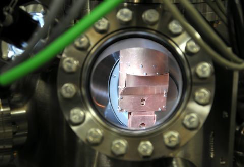
ARPES at Diamond offers a powerful platform for exploring the electronic structure of materials and their surfaces and interfaces. With high surface sensitivity and precise momentum mapping, our VUV ARPES capabilities are particularly well‑suited to samples with layered structures and those with preferential cleavage planes. The technique is ideal for exploring exotic ground states ‑ such as unconventional superconductors, solids with charge and spin density wave systems, excitonic insulators, and non‑Fermi liquids. Equally, it can be used to probe heterostructures and devices of 2D materials.
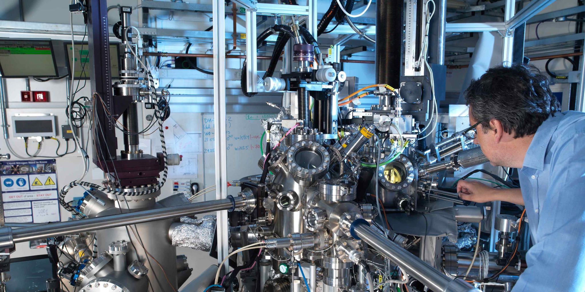
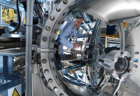
What sets Diamond apart is not just the advanced technology available, but the support behind it. Our expert scientists offer a range of services and flexible access options to help you design and execute your experiments efficiently. Whether you're new to ARPES or an experienced user, we’re here to ensure you get the most from your beamtime.
The beamline supports a wide array of measurements, including ARPES band and Fermi surface mapping to probe electronic band dispersion near the Fermi level, and the Fermi surface itself. Spectral function spectroscopy enables insights into the interaction between photo-holes and the evolving electronic and vibronic structure of your sample. For spatially resolved studies, nano-ARPES allows imaging of grains and domains in natural or artificial structures at micro- and nanometric scales, or selective illumination of specific micro- and nano-domains.