____________________________________
Industrial Liaison Group:
Tel: +44 (0) 1235 778797
E-mail: [email protected]
In theory, sufficient energy reaches the earth’s surface from the sun to meet all of our foreseeable energy needs in a sustainable manner. In practice, the best currently available technology for converting solar energy into electricity – the silicon photovoltaic cell - is very expensive and intrinsically difficult to manufacture on a large scale. Organic based photovoltaics (OPV) that can be manufactured using environmentally friendly materials in low temperature, low cost continuous processes could make a significant contribution to total energy demands.
One new class of OPVs is based on blends of semi-conducting polymers. As the polymers are coated onto the flexible substrates, the molecules self-assemble to form a complex composite material. It has become clear that the performance of the polymer photovoltaic films is very sensitive to variations in the processing conditions in which the devices are made. It is believed that processing conditions influence nanoscale structure and the resulting performance is strongly influenced by the nanoscale structure but in situ measurements of the structural evolution during processing are needed to understand this effect.
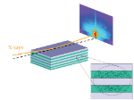
Real time in situ studies of the changes in morphology during the coating process itself, were monitored with X-ray diffraction techniques using Diamond beamlines I22, I16 and I07. During the experiment, the substrate was coated with the polymer solution and the drying and self-organisation processes were characterised by grazing incidence X-ray diffraction (GIXD) and grazing incidence small angle X-ray scattering (GI-SAXS). Grazing incidence diffraction probes the nanoscale structure of thin films and is ideally suited to the investigation of these complex composite materials.
The experiments allowed the researchers to gain an insight into the mechanism by which the processing conditions can affect the resulting nanoscale structure of the organic photovoltaic films. Understanding the relationship between the processing conditions and the structure will lead to design control of the materials to give the optimum morphology for the most efficient photovoltaic device performance.


“Using a range of instruments at Diamond enabled us to monitor structural changes within the polymer photovoltaics during processing in real time. These studies are essential to inform the design of large scale manufacturing processes to produce the next generation of efficient and environmentally friendly solar cell technology.”
Prof. David Lidzey, University of Sheffield

Diamond Light Source is the UK's national synchrotron science facility, located at the Harwell Science and Innovation Campus in Oxfordshire.
Copyright © 2022 Diamond Light Source
Diamond Light Source Ltd
Diamond House
Harwell Science & Innovation Campus
Didcot
Oxfordshire
OX11 0DE
Diamond Light Source® and the Diamond logo are registered trademarks of Diamond Light Source Ltd
Registered in England and Wales at Diamond House, Harwell Science and Innovation Campus, Didcot, Oxfordshire, OX11 0DE, United Kingdom. Company number: 4375679. VAT number: 287 461 957. Economic Operators Registration and Identification (EORI) number: GB287461957003.