Lead-free piezoelectric materials are rapidly gaining interest amongst research groups as the environmental concerns regarding the disposal of toxic, lead-based materials continues in electronic applications. The industry standard, lead zirconate titanate (PZT) is the most widely used piezoelectric today and finds uses in sensor and actuator applications throughout a multitude of high-tech industries,1 with a market value exceeding $10 billion annually.2 Key markets include medical ultrasound, diesel fuel injection, ink-jet printing and optics. PZT contains up to 60% lead by weight and European regulations now exclude the use of most lead-containing materials in electronic and electrical devices, such as solder. Currently, piezoelectric ceramics are exempt. This classification is reviewed regularly and is due for review again in 2012. Piezoelectric materials are typified by their ability to generate a transient current when pressure is applied to two opposing surfaces, and vice-versa.
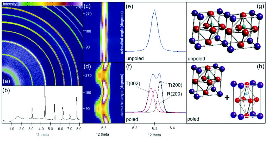
Figure 1(a): directionally dependant diffraction data captured as Debye-Scherrer rings. (b) Integration of raw data to produce a two dimensional diffraction plot. (c) Image of the (200) peak at zero field, no splitting is observed. (d) Image of the ring captured at high field. Contributions from the (002) peak is present. (e) Resulting integrated pattern for the (200) peak at zero field. (f) Resulting integrated pattern for the (200) and (002) peaks at high field. (g) & (h) crystal structures for zero field (rhombohedral) and high field (rhombohedral and tetragonal) conditions.
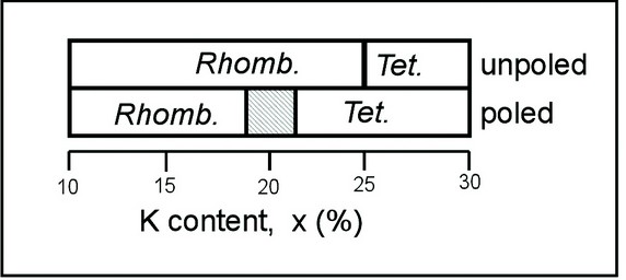
A crystallographic phase boundary has been reported in KNBT at x = 0.2,3, 4 and a maximum in piezoelectric activity and dielectric constant is observed at this point. Hitherto, X-ray diffraction of powders and ceramics have been unable to explain why x = 0.2 is the most piezoelectrically active; no phase boundary has been directly observed, and no focus has been given to the underlying structural mechanism which promotes the enhancements.
Figure 2: Phase diagram of unpoled and poled KNBT, the hashed area represents a mixed phase region induced by the application of an applied field.
The Extreme Conditions beamline (I15) at Diamond Light Source enabled us to successfully design and execute a novel experiment which involved applying a large electric field to a sample in-situ. Standard laboratory X-ray equipment does not offer sufficient penetration depths to be able to perform this type of experiment on ceramics; the data collected from the surface is modified by effects such as strain, and does not provide a true representation of the bulk material – only by probing the crystallography of the bulk can one directly correlate with other measurements such as the piezoelectric activity.
Bar shaped ceramic samples measuring nominally 1 x 1 x 5 mm were fabricated using a standard mixed oxide processing route at the Institute for Materials Research, University of Leeds. The bars were highly dense (>95% of theoretical density) and were made suitable for diffraction experiments by applying silver electrodes to two opposing faces of the bar. The high energies available on I15 were able to penetrate through samples of this thickness. The test specimens were placed in a custom built rig, allowing submersion in silicone oil to prevent electrical breakdown through air.
A highly intense beam of X-rays approximately 57 keV (? = 0.21568 Å) with a spot size 100 x 100 µm was incident on the sample which allowed diffraction data to be collected at all angles to the applied field simultaneously5.
Figure 1 (a): shows a quarter of the raw diffraction data captured as Debye-Scherrer rings on a MAR345 solid state image detector. A “cake” (solid angle of 10° from the origin) was then integrated to yield a conventional intensity vs. 2? plot (b), in a direction both parallel and perpendicular the applied electric field vector.
When the material was electrically poled, there was a visible difference in the appearance of the Debye-Scherrer rings; this was due to the splitting of the rings as the material transformed. The difference in the (200) ring between an unpoled (c) and poled (d) ceramic is stark. It can be seen that there is a directional dependence of the splitting indicated by the asymmetric nature of the ring in (d). Figures 1 (e) and (f): show the resultant intensity - 2? plots of the (200) peak for an unpoled and poled ceramic respectively, in the direction of the electric field. The crystal structure before and after application of an electric field is shown in Figures (g) and (h) respectively; note that the distortions are greatly exaggerated. A transformation from rhombohedral to a mixture of rhombohedral and tetragonal is apparent.
By studying this and other compositions in the KNBT system, we have created a phase diagram for both poled and unpoled materials seen in Figure 2. Using this construct, we are able to show that that the composition x = 0.2 is unique, comprising tetragonal and rhombohedral forms when poled explaining the enhancement in piezoelectric properties at this point. All other compositions are either single phase tetragonal or rhombohedral in the range x = 0.1 to
x = 0.4.
In conclusion, we are able to show using in-situ experiments why an enhancement in properties is piezoelectric activity is observed at x = 0.2, in the material KNBT, a potentially important lead free piezoelectric material. Only this composition shows coexistence of both rhombohedral and tetragonal phases when poled.