Extending the longevity of perovskite solar cells for cheaper solar energy
May 25, 2022
May 25, 2022
Diamond’s Nanoprobe beamline I14 and the electron Physical Science Imaging Centre (ePSIC) were used by a multidisciplinary team of researchers to gain new insight into the perovskite materials that hold so much potential in the field of optoelectronics. Focusing on structural changes that can lead to degradation, the Diamond instruments were part of a suite that enabled the group to observe the nanoscale properties of thin films of perovskite materials and how they change over time under solar illumination. The research, recently published in Nature, could significantly accelerate the development of long-lasting, commercially available perovskite photovoltaics.

Perovskite materials offer a cheaper alternative to silicon for producing solar cells and also show great potential for other optoelectronic applications, such as energy efficient LEDs and X-ray detectors.
The metal halide salts are abundant and much cheaper to process than crystalline silicon. They can be prepared in a liquid ink that is simply printed to produce a thin film of the material.
While the overall energy output of perovskite solar cells can often meet or – in the case of multi-layered, so-called ‘tandem’ devices – exceed that achievable with traditional silicon photovoltaics, the limited longevity of the devices is a key barrier to their commercial viability.
A typical silicon solar panel, like those you might see on the roof of a house, typically lasts about 20-25 years without significant performance losses.
Because perovskite devices are much cheaper to produce, they may not need to have as long a lifetime as their silicon counterparts at least to enter some markets – but to fulfil their ultimate potential in realising widespread decarbonisation, cells will need to operate for at least a decade or more. Researchers and manufacturers have yet to develop a device with similar stability to silicon cells.
Now, researchers at the Department of Chemical Engineering and Biotechnology (CEB) and Cavendish Laboratory at the University of Cambridge, together with the Okinawa Institute of Science and Technology (OIST) in Japan, have discovered that the defects that limit perovskite efficiency are also responsible for structural changes in the material that lead to degradation.
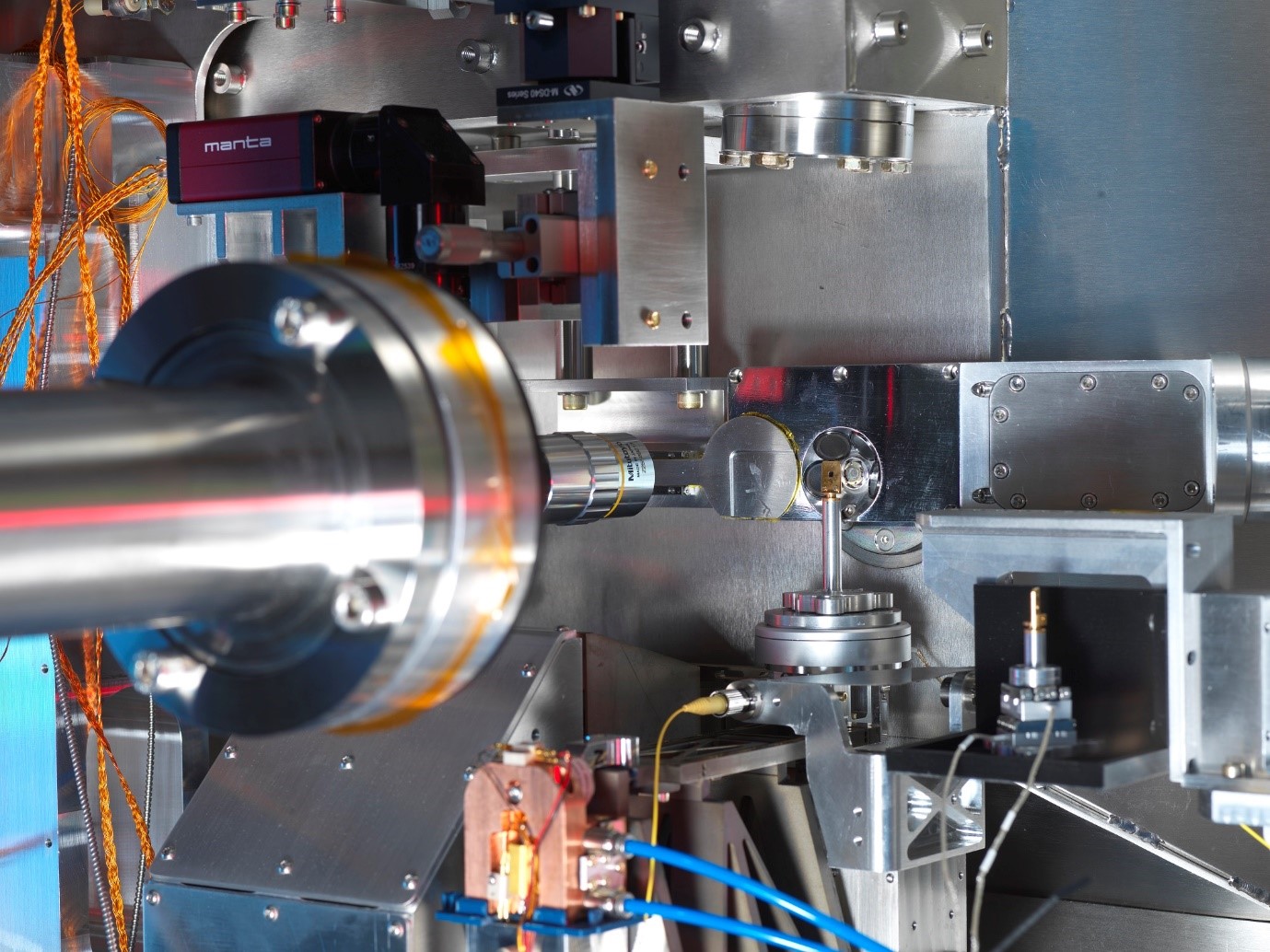
Using a multimodal toolkit of high spatial-resolution techniques, in collaboration with Diamond’s Nanoprobe beamline and electron Physical Sciences Imaging Centre (ePSIC), and the Department of Materials Science and Metallurgy in Cambridge, the group were able to observe the nanoscale properties of these thin films and how they change over time under solar illumination.
Previous work by the team using similar spectroscopic techniques has shone light on the defects that cause deficiencies in the performance of perovskite photovoltaics – so-called carrier traps.
Dr Stuart Macpherson, Postdoctoral Researcher at the Cavendish Laboratory says:
Illuminating the perovskite films over time, simulating the aging of solar cell devices, we find that the most interesting dynamics are occurring at these nanoscopic trap clusters.
We now know that the changes we see are related to photodegradation of the films. As a result, efficiency-limiting carrier traps can now be directly linked to the equally crucial issue of solar cell longevity.
Dr Tiarnan Doherty, an Oppenheimer Research Fellow at CEB and Murray Edwards College explains:
It’s pretty exciting because it suggests that if you can address the formation of these surface traps, then you will simultaneously improve performance and the stability of the devices over time.
By tuning the chemical composition, and how the perovskite film forms, in preparing the devices, the authors show that it’s possible to control how many of these detrimental phases form and, by extension, how long the device will last.
Doherty explains:
The most stable devices discussed in the literature seem to be serendipitously lowering the density of detrimental phases through subtle compositional and structural modifications. We’re hoping that this paper reveals a more rational, targeted approach for doing this and achieving the highest performing devices operating with maximal stability.
The group are optimistic that their latest findings will bring us closer still to the first commercially available perovskite photovoltaic devices.
Dr Sam Stranks, University Assistant Professor at the University of Cambridge and corresponding author on the paper explains:
Perovskite solar cells are on the cusp of commercialisation, with the first production lines already producing modules. From this work, we now understand that any residual unwanted phases – even tiny nanoscale pockets remaining from the processing of the cells – will be very bad news for longevity of perovskite solar cells. The manufacturing processes therefore need to incorporate careful tuning of the structure and composition across large area to eliminate any trace of these unwanted phases – even more careful control than is widely thought for these materials. This is a great example of fundamental science directly guiding scaled manufacturing.
Dr Keshav Dani, Associate Professor at OIST in the Femtosecond Spectroscopy Unit says:
It has been very satisfying to see the novel, multimodal, nanoscale approaches, that we've developed at OIST and Cambridge over the past several years, provide direct visuals of these tiny residual unwanted phases, and how they change over time. The hope remains that these techniques will continue to reveal the performance limiting aspects of photovoltaic devices, as we work towards studying operational devices.
Macpherson concludes:
Another strength of perovskite devices is that they can be made in countries where there’s no existing infrastructure for processing monocrystalline silicon. Silicon solar cells are cheap in the long-term but require a substantial initial capital outlay to begin processing. But for perovskites, because they can be solution processed and printed so easily, using far less material, you remove that initial cost. They offer a viable option for low- and middle-income countries looking to transition to solar energy.
To find out more about I14 or discuss potential applications, please contact Principal Beamline Scientist Julia Parker: [email protected]. For details about ePSIC, please contact Principal Electron Microscopist Chris Allen: [email protected].
Macpherson, S. et al. Local Nanoscale Phase Impurities are Degradation Sites in Halide Perovskites. Nature (2022). DOI: 10.1038/s41586-022-04872-1

Diamond Light Source is the UK's national synchrotron science facility, located at the Harwell Science and Innovation Campus in Oxfordshire.
Diamond Light Source Ltd
Diamond House
Harwell Science & Innovation Campus
Didcot
Oxfordshire
OX11 0DE
Copyright © Diamond Light Source. Diamond Light Source® and the Diamond logo are registered trademarks of Diamond Light Source Ltd
Registered in England and Wales at Diamond House, Harwell Science and Innovation Campus, Didcot, Oxfordshire, OX11 0DE, United Kingdom. Company number: 4375679. VAT number: 287 461 957. Economic Operators Registration and Identification (EORI) number: GB287461957003.