From Theory to Confidence: Building Trust in Twistronics Models
Feb 23, 2024
Feb 23, 2024
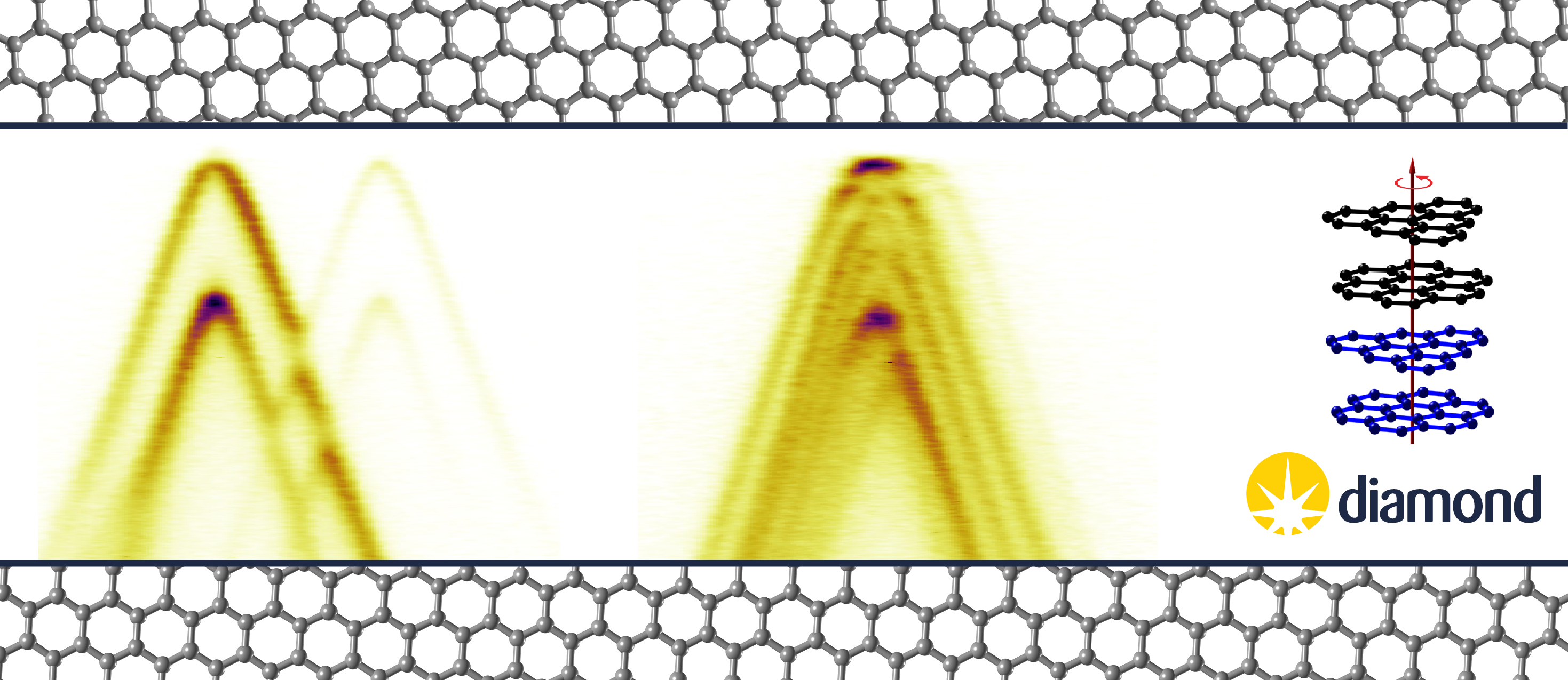
A single sheet of graphene, composed of a single layer of carbon atoms in a hexagonal pattern, is a semimetal. However, adding a second sheet of graphene, twisted at a slight angle to the first, can give rise to very different electronic properties, depending on the angle. At the 'magic' angle of about 1.1°, for example, a twisted bilayer sheet of graphene is a superconductor. The same effect is seen in other 2D materials, giving rise to a new field of study - twistronics - seeking to both understand and exploit the relationship between twist angles and novel electronic properties. In work recently published in Nano Letters, researchers from the University of Warwick and the National Graphene Institute at the University of Manchester used spatially-resolved angle-resolved photoemission spectroscopy (ARPES) on Diamond's I05 beamline to study the twist-dependent band structure of twisted-bilayer, monolayer-on-bilayer, and double-bilayer graphene. Their results show good agreement between experimental measurements and theoretical simulations, confirming that the models can be used to explore the electronic band structure and emergent transport and optical properties of twisted-few-layer graphenes.
Prof Neil Wilson at the University of Warwick opens by noting that;
Twistronics is a new concept in 2D materials, in condensed matter physics. When you have two atomically thin layers next to each other, their properties depend on the twist angle between them. This happens because of changes to the electronic structure, and there has been a huge amount of research on twistronics - putting two layers together at different twist angles and seeing what happens to the optical properties and electrical properties. You're working with two very small pieces of 2D material stacked on top of each other, typically only a few micrometres across, which is fine for optical measurements and electrical transport measurements. However, that makes it extremely challenging to study the electronic structure directly.
To get a good look at the electronic structure of these exciting materials, Prof Wilson's group at the University of Warwick worked with researchers from the National Graphene Institute and Diamond's I05 beamline. Prof Roman Gorbachev's group at the National Graphene Institute is a world leader in fabricating these complex samples.
Senior Beamline Scientist Matthew Watson explains;
Angle-resolved ARPES allows us to measure directly the electronic structure of the 2D materials. It allows us to determine both the energy and momentum of the electrons within the material, which gives us directly the electronic structure which underpins the optical properties and the transport properties. And the I05 nano-branch endstation delivers spatially-resolved ARPES from ultra-small spots, on the micrometre length scales we have in these 2D samples.
Lead author James Nunn, at the time a joint PhD student at Diamond and the University of Warwick, led the data acquisition and the first level data analysis.
Also involved in this project were Prof Vladimir Falko and his group at the National Graphene Institute, world leaders in the theory of electronic structure of these 2D materials.
Scientists rely on theoretical models to predict electronic structure, to explain the optical and transport phenomenon and to develop new geometries. For twistronics, the models are very complex, because of the number of atoms involved in the moiré patterns that arise when two similar patterns interact to cause an interference pattern.
Prof Wilson said;
Our experiments at Diamond allowed us to work out under which conditions the theoretical models are applicable. Using ARPES, we thoroughly tested the different models and showed that - for most twist angles - a comparatively simple model is applicable. Close to the magic angle, however, you need to account for more complicated effects. The key output for the 2D material field was testing these models so people can have confidence in when and how they can be used. But it is also a demonstration of what is now possible by ARPES. So I would say that most of this data would not have been possible to acquire a few years ago. It's only kind of the recent advances that have made this possible.
Principal Beamline Scientist Cephise Cacho added;
This was a very exciting project for I05, which brought together world-leading groups based in the UK. At Diamond, we pride ourselves on supporting our user community, but this was a great opportunity to go beyond that and really collaborate on the science. We are continuing to develop the collaboration, and to work on twistronics and 2D materials.
To find out more about the I05 beamline or discuss potential applications, please contact Principal Beamline Scientist Cephise Cacho: [email protected]
Nunn JE et al. ARPES signatures of few-layer twistronic graphenes. Nano Letters (2023). DOI:10.1021/acs.nanolett.3c01173.

Diamond Light Source is the UK's national synchrotron science facility, located at the Harwell Science and Innovation Campus in Oxfordshire.
Diamond Light Source Ltd
Diamond House
Harwell Science & Innovation Campus
Didcot
Oxfordshire
OX11 0DE
Copyright © Diamond Light Source. Diamond Light Source® and the Diamond logo are registered trademarks of Diamond Light Source Ltd
Registered in England and Wales at Diamond House, Harwell Science and Innovation Campus, Didcot, Oxfordshire, OX11 0DE, United Kingdom. Company number: 4375679. VAT number: 287 461 957. Economic Operators Registration and Identification (EORI) number: GB287461957003.