Atomically thin clays and micas offer super speedy ion exchange
Oct 20, 2021
Find out about upcoming events and webinars, and watch past events.
You can also explore Diamond by using our interactive map and discover the synchrotron, beamlines and much more.
Oct 20, 2021
Ion exchange is a reversible process where an ion in solution replaces a different ion with the same charge on an insoluble solid. This type of reaction has many applications, including softening or demineralising water, purifying chemicals and filtering substances. Although clays and micas are widely used as selective membranes, the ion exchange process in atomically thin clays has remained largely unexplored. In work recently published in Nature Materials, research led by the University of Manchester has used high-resolution scanning transmission electron microscopy to demonstrate that ions diffuse 10,000 times faster inside atomically thin clays than in bulk clay crystals. The results suggest that switching to ultra-thin clays for membranes could dramatically improve performance in applications from fuel cells to desalination.
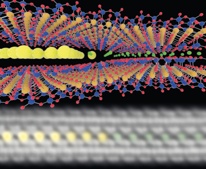
Clays and micas are stacks of crystal layers a few atoms thick, with ions such as K+ or Mg2+ in the interlayer space. Ion exchange allows different ions to penetrate the interlayer space in a controllable way (Fig. 1).
It is possible to separate the crystal layers - mechanically or chemically - to create ultra-thin materials. These 2D materials can then be layered into laminate membranes and composites in a similar way to graphene oxide. In these fabricated materials, the crystal surface charge controls water and ion transport through the interlayer channels. Advances in fabrication methods mean we can now produce model structures with precise control of the number and composition of layers and the stacking geometry.
However, although this offers great potential for applications such as osmotic power generation, ion selective transport or solvent filtration, ion exchange in these atomically thin clays and micas is not well understood.
A team led by Professor Sarah Haigh and Dr Marcelo Lozada-Hidalgo used advanced aberration-corrected scanning transmission electron microscopy (STEM) to investigate the dynamics of ion exchange in atomically thin (Fig. 1) and artificially restacked clays and micas (Fig. 2). The advantage of using STEM over more common techniques such as atomic force microscopy or X-ray measurements is that it reveals the local binding environment of exchanged ions with sub-ångström resolution. Using STEM to observe ion exchange processes in atomically thin layered and restacked clays allowed the team to see substantially larger ion diffusion constants and moiré effects on ion dynamics.
The team chose to use caesium (Cs+) for their ion exchange experiments for two reasons. Firstly, caesium's large atomic number makes it easily visible in annular dark field (ADF) STEM images. And an improved understanding of the diffusion of radiocaesium (caesium-137) through clays and micas will inform environmental clean-up after nuclear contamination.
Professor Sarah Haigh, explains:
We do a lot of the microscopy in our own lab, but the microscope at ePSIC allows us to see both the heavy elements and the light elements.
We simultaneously take a dark field image that shows us where the exchanged ions are, and a bright field image that tells us about the underlying lattice. That's extremely important because it allows us to correlate the position of the exchanged ions relative to the underlying lattice. It also has incredible imaging resolution even at very low accelerating voltage, which helps reduce electron beam damage to the sample.
The team found that the ion diffusion coefficient for the interlayer space of atomically thin samples was up to 104 times larger than in bulk crystals, allowing ions to diffuse 10,000 times faster. Using complementary atomic force microscopy measurements, they showed that this effect likely arises because the long-range (van der Waals) forces that bind the 2D clay layers are weaker in thin layers. This allows more swelling, effectively giving the ions more space to move quickly.
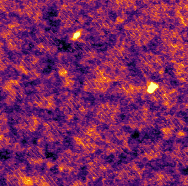
The research team found, unexpectedly, that when they added a rotational offset or misalignment between layers, the caesium ions arranged themselves in clusters (or islands), the size of which depends on the angle between the layers. The presence of these moiré superlattices will allow us to use stacked 2D materials to create unique nanoscale interlayer environments that can accommodate ions or molecules.
The technique the team developed to investigate these clays and micas is likely to have much broader application. The team are now working to develop it from taking "snapshots" to producing "movies".
Prof Haigh, added:
One of the problems with atomic resolution imaging of these materials is that they are extremely sensitive to electron radiation.
As a result, it's often only possible to take one or two STEM images before the crystal lattice is damaged. One of the next steps for this research is to use a less sensitive system, take more images and see the ion exchange process processing frame-by-frame. The crystals we worked with here were very high-quality, defect-free crystals. Adding defects often introduces exciting effects, so we also want to investigate what happens to the ion exchange in more defective crystals.
The electron Physical Science Imaging Centre (ePSIC) is a national facility for aberration-corrected electron microscopy. To find out more about ePSIC or discuss potential applications, please contact Principal Electron Microscopist Chris Allen: [email protected].
Zou Y.-C. et al. Ion exchange in atomically thin clays and micas. Nature Materials (2021): 1-6. DOI:10.1038/s41563-021-01072-6.

Diamond Light Source is the UK's national synchrotron science facility, located at the Harwell Science and Innovation Campus in Oxfordshire.
Diamond Light Source Ltd
Diamond House
Harwell Science & Innovation Campus
Didcot
Oxfordshire
OX11 0DE
Copyright © Diamond Light Source. Diamond Light Source® and the Diamond logo are registered trademarks of Diamond Light Source Ltd
Registered in England and Wales at Diamond House, Harwell Science and Innovation Campus, Didcot, Oxfordshire, OX11 0DE, United Kingdom. Company number: 4375679. VAT number: 287 461 957. Economic Operators Registration and Identification (EORI) number: GB287461957003.