Chris Nicklin, Village Coordinator
The Surfaces and Interfaces village consists of five operational beamlines: the Angle Resolved Photoelectron Spectroscopy (ARPES) beamline (I05), the Nanoscience beamline (I06), the Surface and Interface Diffraction beamline (I07), the Surface and Interface Structural Analysis (SISA) beamline (I09) and BLADE, the Beamline for Advanced Dichroism Experiments (I10). These facilities offer a very comprehensive range of techniques to users that enable them to determine the physical and electronic structure of their samples using diffraction and spectroscopic techniques. Nanostructures or the atomic structure of well-ordered samples can be accurately measured by a number of methods, depending on the parameters to be probed and the environment of the sample. More details of the structural methods available in the village are given in the developmental updates section later in this report. The electronic (or magnetic) structure can be probed with very high resolution using techniques including: X-ray Photoelectron Spectroscopy (XPS), X-ray Absorption Spectroscopy (XAS) or X-ray Magnetic Circular, or Linear, Dichroism (XMCD or XMLD). These can, for example, provide detailed mapping of the band structure, measure the electronic core levels, enable spatially resolved measurements from nanostructures or probe buried interfaces using hard X-ray beams.
Electronic structure and spin-valley-layer coupling in the strong spin-orbit semiconductor WSe2
 Spintronics is a novel field of electronics that exploits electron spins with the hope of developing faster, more energy-efficient devices. Materials with a strong coupling between the spin and orbital motion of an electron, so-called spin-orbit coupling, represent a promising route to achieve such aims. A compound expected to have strong spin-orbit coupling, the layered semi-conductor WSe2, was previously studied at the MAX-lab synchrotron using spin- and angle-resolved photoemission spectroscopy.
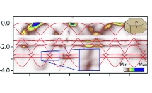
The fate of charge density wave order while superconductivity is enhanced by light in the high-TC cuprate YBa2Cu3O6.6
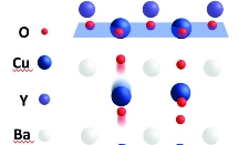 The crucial challenge in the field of superconductivity is the development of unconventional high-temperature superconductors, which display superconducting properties at temperatures above the boiling point of liquid nitrogen (77 K). Yttrium barium copper oxide was the first material to show superconductivity above 77 K with a critical temperature, Tc, of 92 K. Two competing ordering features underpin the physics of superconductors: charge ordering and phase coherence, with the balance influenced by magnetic fields and pressure.
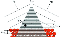
Where do metals diffuse inside a nanoparticle?
 Nanoparticles exhibit excess surface free energy and structural instabilities, which leads to interesting chemical and physical properties that can be exploited in fields such as semiconductors and catalysis. The question of atomic diffusion in nanoparticles, a thermallyactivated mixing process, has remained unanswered for many years due to an inability to image the crystals in three dimensions in their ‘as-grown’ in situ environment.
Surface reactions studied with X-ray standing waves
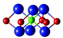
 Large π-conjugated molecules have been studied for many years for their optical properties. Their recent usage in organic electronics such as organic LEDs has increased interest in their surface science. To optimise device function and efficiency it is crucial to understand the interactions occurring at the organic-metal interface and how these affect electronic and structural properties. Porphyrin consists of a carbon macrocycle containing four nitrogen atoms that can bind a metal ion in the central pocket of the molecule.
Are the Cr dopants in the Bi2Se3 topological insulator divalent or trivalent?
 A toplogical insulator (TI) behaves as an insulator in its interior whilst conducting electrons along the surface of the material. When doped with magnetic elements, TIs exhibit exotic quantum and magneto-electrical properties that offer the prospect of their use in spintronic materials for microelectronics and data storage. The most successful ferromagnetic TI discovered to date is chromiumdoped (Bi,Sb)2(Se,Te)3 as it combines ferromagnetic ordering with acceptable levels of bulk doping.
It has long been known that many functional properties of a material are linked to its specific structure. These relationships may occur at different length scales, for example, some rely on the microstructure, such as how the size of polycrystalline grains in engineering materials can affect their strength. However, many properties are linked to the atomic structure of the material and this becomes even more important at the surface of a material or at an interface between components where the environment is different from the interior of the sample. A number of different phenomena can occur, including surface relaxation or reconstruction, where the atoms in the outer layers move in directions either perpendicular or parallel to the surface (or both). The delicate balance of energy at the surface or interface can lead to other significant changes such as surface alloying (from constituents that do not readily form bulk alloys), faceting or changes in the chemical state of the surface. Such changes at the surface have led to a wide range of real technological devices; for example, the enhancement of the magnetoresistance in thin films has led to the development of very sensitive read heads for magnetic recording, while improved catalysts have been developed by tailoring the size of particles on a specific support. Diamond has a number of techniques available to provide information about the structure of the surface or interface at the atomic scale or for nanostructures supported on a sample, where the high surface area to volume ratio can have a significant effect on the properties.
Imaging techniques such as Photoelectron Emission Microscopy (PEEM) provide a real space view of nanostructures with a resolution of typically 30 nm, for samples held in ultrahigh vacuum (UHV). PEEM uses a complex series of electron optics to form an image of the emitted photoelectrons, resulting from the impinging soft X-ray beam. The data collected provides a direct link between the structure and the spectroscopic information from the distribution of photoelectrons providing, for example, chemical sensitivity in the distribution of elements at a surface. The measurements available at beamline I06 allow additional versatility as the X-rays are provided by an Apple-II undulator which enables the polarisation to be selected (e.g. horizontal linear, vertical linear or circular). Contrast mechanisms, such as dichroism in the difference spectra, can be used to form images that show magnetic domains and their response to external stimulus. The PEEM on the Nanoscience beamline (I06) has been used to study the local magnetisation in nickel films on ferroelectric BaTiO1 and combined spectroscopy and microscopy on ultrathin ceria films2, amongst many others.
- Figure 1: The RASOR soft X-ray diffractometer available at beamline I10.
Hard X-ray scattering methods can also be used to understand the structure of nanoparticles. Grazing Incidence Small Angle X-ray Scattering (GISAXS) is a surface sensitive probe that detects the scattering close to the direct beam, to establish parameters such as particle shape and size, interparticle interactions and long range order. The Surface and Interface Diffraction beamline (I07) has a large area detector that can be positioned 1.5-3.0 m from the sample to enable such measurements of particles up to approximately 50 nm in size. This detector can also be mounted closer to the sample to enable Grazing Incidence Wide Angle X-ray Scattering (GIWAXS) that is sensitive to smaller length scales. GIWAXS has proven particularly popular in the study of organic photovoltaic (OPV) systems3. Beamline I07 is dedicated to the determination of surface and interface structures through hard X-ray scattering and in addition to GISAXS and GIWAXS, is able to perform X-ray Reflectivity (XRR) to provide information on a layer structure in the direction perpendicular to the surface, or Grazing Incidence X-ray Diffraction (GIXD) where the lateral structure of a well ordered layer can be determined. The full structure of well-ordered surfaces can be established with very high resolution using surface X-ray diffraction (SXRD) to measure, so called, crystal truncation rods (CTR’s) . The use of hard X-rays (8-30 keV) in all of these techniques means that although they can be performed in ultrahigh vacuum, they are not limited to it, and beamline I07 has been used for example, to study battery materials during charging, the buried interface between two misaligned silicon crystals, and the ordering of molecules on water surfaces.
A range of other techniques are available at the Surface and Interface Structural Analysis (SISA) beamline (I09). It is able to provide a wide range of measurements on samples held in UHV as it has both a soft X-ray beam and a hard X-ray beam available with the sample held in the same position. Photoelectron Diffraction (PhD) detects the spatial distribution of emitted photoelectrons, which can be related to the local atomic environment of the emitting atom and therefore to establish nearest neighbour distance, atom type and registry with the underlying sample. Also available at I09, X-ray Standing Waves (XSW) is a technique where the X-ray energy is tuned to set up a standing wave of the same wavelength as the distance of some specific planes in a single crystal sample. If there is a surface reconstruction or adsorbate in a particular site then the detected intensity as the energy is scanned exhibits a profile that is dependent on the position of the outer layer atoms. Very accurate positional information can be extracted by triangulation using different atomic planes. I09 is able to relate these structural parameters to changes in the electronic structure through X-ray Photoelectron Spectroscopy (XPS), using both soft X-rays and hard X-rays.

Figure 3: In situ UHV growth chamber on beamline I07 enables surface X-ray diffraction measurements of well-ordered surfaces and interfaces.
BLADE, the Beamline for Advanced Dichroism experiments (I10), can also provide structural information through soft X-ray diffraction using the RASOR end station. This is a diffractometer that allows reflectivity (theta – 2theta) and diffuse scattering measurements using soft X-rays, which has proven to be very useful in the study of multilayer structures. BLADE, like I06, is able to change the polarisation of the incident X-ray beam4 which has been a very powerful probe in the study of both magnetic multilayers and single crystal system such as multiferroics5. Moreover, the successful installation of two CCD cameras has enabled the successful measurement of X-ray photon correlation spectroscopy from artificial spin ice as well as the possible detection of topological states.
This article has highlighted some of the techniques available at Diamond that can help to determine the structure at the surface, interface or nanostructured sample. In addition, there are numerous support techniques available (both offline and at other beamlines) that can provide complementary information.
Reference:
1. Ghidini M. et al. Perpendicular Local Magnetization Under Voltage Control in Ni Films on Ferroelectric BaTiO3 Substrates. Adv. Mat. 1460-5 (2015).
2. Grinter D. et al. Characterising Ultrathin Ceria Films at the Nanoscale: A Combined Microscopic Approach. J. Elect. Spect. and Rel. Phen. 195 13 – 17 (2014).
3. Agostinelli T. et al. Real-Time Investigation of Crystallization and Phase-Segregation Dynamics in P3HT:PCBM Solar Cells During Thermal Annealing. Adv. Func. Mat. 21, 1701-1708 (2011).
4. Wang H. et al. Complete polarization analysis of an APPLE II undulator using a soft X-ray polarimeter. J. Synchrotron Rad. 19, 944-948 (2012).
5. Hearmon A. J. et al. Magnetic fan structures in Ba0.5Sr1.5Zn2Fe12O22 hexaferrite revealed by resonant soft x-ray diffraction. Phys. Rev. B 88, 174413 (2013).
The village also has one facility under construction. B07, the Versatile Soft X-ray (VERSOX) beamline, will complement the range of experiments that can be undertaken by enabling spectroscopic measurements on samples held in non-vacuum environments. This will bring a deeper understanding to science areas such as catalysis, pharmaceuticals and biomaterials under realistic conditions or atmospheric chemistry. Construction work has started and the first users are expected by the end of the year. Concurrently, one of the end stations is being constructed and commissioned on the soft X-ray branch of I09 to enable a fast transfer to B07 when available.
The areas of science covered by the village have continued to grow; in particular there has been a significant increase in the number of studies on oxide samples, including complex transition metal oxides or actinide oxides. Transition metal dichalcogenide samples also remain much studied due to the interesting electronic effects that they exhibit, in particular when doped with other elements. The village has also welcomed users interested in areas as diverse as organic photovoltaics, phase changes in rechargeable battery materials, protein interaction at the lipid-water interface or in situ studies of molecular adsorption on single crystal samples. This year, the highlighted publications show a wide variety of techniques and materials with results all published in high quality journals. A brief summary of those reports is given below.
Beamline I05 has produced many high quality publications since becoming fully operational this year, including the highlighted work from Phil King's group in St. Andrews. They report on the layered semiconductor WSe2, which demonstrates an interesting spin-orbit coupling within each layer. The overall symmetry of the system is maintained by a 180° rotation between the layers that is confirmed by the close agreement of the photon energy-dependent ARPES measurements with the theoretically calculated electronic structure. The authors discuss the results in the context of spintronic devices, where control of the electron spin could be used to create faster, or more energy efficient, devices.
I06 was the first operational beamline in the village and continues to provide a number of different techniques using the polarised soft X-ray sources, including time resolved pump-probe methods using the lasers available at the beamline. Foerst (Max Planck Institute for the Structure and Dynamics of Matter) et al have performed resonant soft X-ray diffraction experiments at I06 to study the link between superconductivity and charge order in the high temperature superconductor YBa2Cu3O6.6. They show how the superconducting state can be enhanced at temperatures just higher than the superconducting critical temperature (Tc), by excitation using mid-infrared femtosecond pulsed light. This is explained in terms of the excitation of particular vibrational modes in the crystal lattice and melting of the charge stripe order. Together with data recorded at the Linac Coherent Light Source (LCLS) in California, details of the dynamics of this process are presented.
Beamline I07 is generally used to determine very accurate structural parameters about well-ordered reconstructions or layered surfaces and interfaces using a number of grazing incidence hard X-ray scattering measurements. Ian Robinson's (UCL) group have now added Bragg Coherent Diffraction Imaging to this list by exploiting the coherent properties of the Diamond source, to image nanoparticles of ~300 nm diameter. They were able to link the technique and the growth capabilities of the ultrahigh vacuum chamber at I07 to study in situ alloying by depositing copper on top of gold nanoparticles, together with subsequent annealing. They show how the copper alloys with the gold by insertion through channels in the nanoparticles. In particular, phase loops were observed indicating the high degree of strain that occurred at the corners and edges of the faceted gold particles.
The SISA beamline (I09) is unique at Diamond in that it enables experiments using both soft X-rays (100eV-2.1 keV) and hard X-rays (2.1-20 keV) to be used on samples held in the same environment and at the same position. This enables combined studies of the atomic structure (using for example X-ray standing waves or photoelectron diffraction) and the electronic structure (e.g. soft or hard X-ray photoelectron spectroscopy). The highlight shows how Alexander Gerlach's (Universität Tübingen) team have used I09 to study the adsorption of large molecules (in this case porphyrin) onto single crystal metal surfaces. Using X-ray standing waves, they were able to establish the adsorption height of the carbon and nitrogen constituents in the adsorbed molecule, showing a slight distortion of the non-metal containing porphyrin. The process of self-metalation, where modest annealing causes incorporation of a metal atom from the substrate into the adsorbate, was investigated showing how the geometry develops by flattening the molecule.
Science related to spintronics is also highlighted in the article from Adriana Figuera-Garcia (Diamond) and co-workers, who have used X-ray magnetic circular dichroism (XMCD) at beamline I10 together with X-ray absorption spectroscopy at beamline B18 to measure the electronic and magnetic structure due to the presence of a dopant (chromium) in a thin film topological insulator (Bi2Se3). The dopant is found to substitutionally replace Bi atoms in the structure, causing a slight distortion in the surrounding lattice. This leads to an unexpected valence in the Cr, which is explained by the covalent nature of the Cr-Se bond. The XMCD measurements highlight differences between the electronic and magnetic structures at the surface of the film and in the bulk.
The Surfaces and Interfaces village continually develops its range of techniques and measurement facilities in consultation with the users. Please get in touch if you would like to discuss any future developments that you would like to see on the beamlines or in any of the extensive offline facilities that are available to users. If you have any questions regarding possible measurements at Diamond or would like advice on how the Surfaces and Interfaces village resources may help with your science programme then please contact [email protected]

Diamond Light Source is the UK's national synchrotron science facility, located at the Harwell Science and Innovation Campus in Oxfordshire.
Diamond Light Source Ltd
Diamond House
Harwell Science & Innovation Campus
Didcot
Oxfordshire
OX11 0DE
Copyright © Diamond Light Source. Diamond Light Source® and the Diamond logo are registered trademarks of Diamond Light Source Ltd
Registered in England and Wales at Diamond House, Harwell Science and Innovation Campus, Didcot, Oxfordshire, OX11 0DE, United Kingdom. Company number: 4375679. VAT number: 287 461 957. Economic Operators Registration and Identification (EORI) number: GB287461957003.