It's a trap! Uncovering defects in next-generation solar panel materials
Oct 21, 2020
Oct 21, 2020
In 2019, the UN reported that the world has made progress towards its Sustainable Development Goal of ensuring that everyone has access to affordable, reliable, sustainable and modern energy.
Nearly 90% of people now have access to electricity, but there are still 840 million people who do not - mainly in rural areas. Energy efficiency continues to improve, and renewable energy is providing more and more of our electricity. For this progress to continue, we need to develop cheaper and more efficient solar panels. However, silicon cells are not very efficient at converting sunlight into electricity (rooftop modules are typically only 20% efficient) and are large, heavy and expensive to manufacture.
Over the last decade, perovskite materials have emerged as promising alternatives to silicon solar cells. They can already achieve a similar efficiency whilst being cheaper and greener to manufacture. However, current perovskite materials still suffer from significant performance losses and instabilities, the cause of which is not well understood.
In work recently published in Nature, a multi-institutional collaboration, co-led by scientists at the University of Cambridge and Okinawa Institute of Science and Technology Graduate University (OIST), has identified the source of these efficiency-limiting defects. Their results will help to increase the efficiency of perovskites solar panels and bring them closer to mass-market production.
In 2009, Japanese scientist Tsutomu Miyasaka and his colleagues discovered that solar cells can be made using halide perovskite materials as the light-harvesting layer. These perovskites are manufactured materials that have the same unique type of crystal structure as calcium titanium oxide. Easy to make by mixing cheap lead halides and organic halides, perovskite inks can be printed into extremely fine layers about 1/100th the thickness of a human hair.
According to Dr Sam Stranks, from the University of Cambridge:
We can strongly absorb almost all wavelengths of sunlight with a perovskite film a hundred times thinner than silicon solar cells. The amount of perovskite ink you'd need to make enough solar panels to power the state of California would only half fill an Olympic swimming pool.
Perovskite materials can also be used in combination with silicon, to make "tandem" solar cells. The perovskite layer harvests blue light, the highest energy visible wavelengths. It lets the rest of the light pass through to the silicon layer below. The combination of two layers allows the panel to more efficiently harvest almost the whole visible spectrum and has the potential to push efficiencies of modules beyond 30%. Tandem cells made from two different perovskite materials, without silicon, can be similarly efficient but also offer opportunities for lightweight and flexible panels.
Unlike silicon, perovskite films only require gentle heating to be defect-free. However, they do still suffer from significant performance losses - particularly in the materials that show the most promise for tandem cells. Research to date has focused on ways to mitigate these losses (e.g. using additives largely by trial and error) rather than understanding their cause.
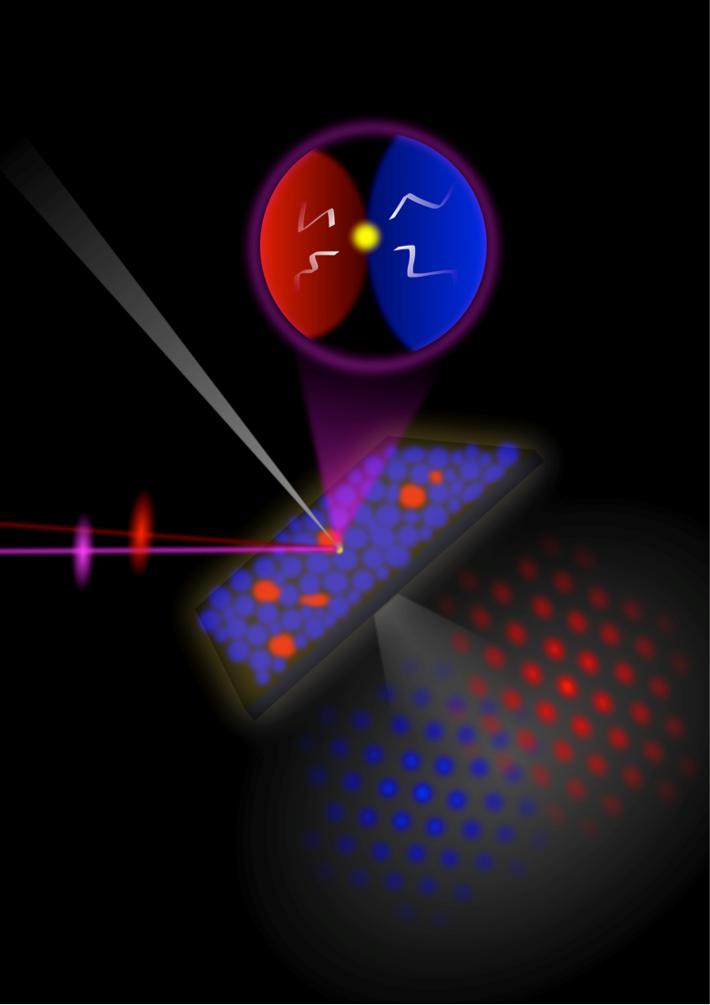
The issue is that certain types of defect present in perovskites can cause "deep traps", areas where charge carriers get stuck and waste their collected energy as heat rather than it being converted into electricity.
In 2015, Dr Stranks and his colleagues published their work investigating the luminescence of perovskites, which shows how well they absorb or emit light1. They found that some areas were bright and luminescent, while other regions were dark and cause power losses.
Meanwhile, Professor Keshav Dani's group at OIST were making movies of how electrons behave in semiconductors after absorbing light2. Dr Stranks proposed a collaboration between the two groups to try and get a better look at the dark regions in perovskites.
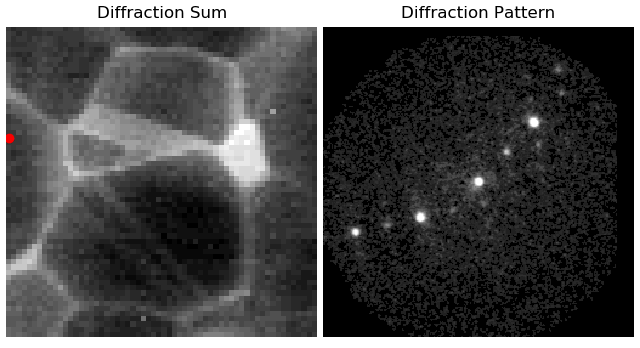
Together, the teams achieved success by correlating the results from a variety of imaging techniques. The team at OIST used photoemission electron microscopy (PEEM) to probe perovskites for the first time. They were able to build up an image of regions that had many deep trap states by monitoring the emission of the trapped electrons from those sites when they probed the material with ultraviolet light.
Correlating the PEEM results with luminescence studies showed that the areas of poor luminescence correspond with traps. This is evidence that they are responsible for the power losses.
Dr Stranks' team worked with Diamond's I14 beamline to carry out X-ray diffraction (XRD) studies on the same samples.
As Dr Stranks explains:
When we started these experiments, I14 was a new beamline, still in its commissioning phase. We developed a great working relationship with the beamline staff and have been able to feed into the development of the beamline. The facilities there are the perfect match for what we needed for our research.
Dr Stranks’ team worked together with Prof Paul Midgley's team to investigate the same samples at the electron Physical Science Imaging Centre (ePSIC) using low-dose scanning electron diffraction (SED) microscopy. Using the same correlation techniques on these two sets of images showed where in the crystal structure the defects occur.
Tiarnan Doherty, a graduate student working in Stranks’ team who was the co-first author of the work, said:
The location of these defects is very interesting. They occur at the interface between normal crystal structure and an area of inhomogeneity, which may turn out to be an impurity. And they only form there. These results are encouraging because they confirm that the traps form during processing and that they could be removed.
It is possible to manage defects using additives or adding in extra layers. The key for commercial production is to find the right balance between optimising efficiency and maintaining the ease of manufacture. This fundamental work will be valuable in finding that balance.
In the meantime, Dr Stranks is looking forward to future experiments on both I14 and ePSIC, applying their multimodal techniques to more 2D semiconductor materials, as well as different halide perovskites that can be used in coloured LEDs and tandem solar panels.
ePSIC is a national facility for aberration corrected electron microscopy. ePSIC was established as a collaboration between Johnson Matthey, the University of Oxford and Diamond Light Source. To find out more about ePSIC, or to discuss potential applications, please contact Principal Electron Microscopist Chris Allen [email protected]. For beamline I14, contact Principal Beamline Scientist Paul Quinn: [email protected].
Doherty TAS, Winchester, et al. Performance-limiting nanoscale trap clusters at grain junctions in halide perovskites. Nature 580, 360–366 (2020). DOI: 10.1038/s41586-020-2184-1.

Diamond Light Source is the UK's national synchrotron science facility, located at the Harwell Science and Innovation Campus in Oxfordshire.
Diamond Light Source Ltd
Diamond House
Harwell Science & Innovation Campus
Didcot
Oxfordshire
OX11 0DE
Copyright © Diamond Light Source. Diamond Light Source® and the Diamond logo are registered trademarks of Diamond Light Source Ltd
Registered in England and Wales at Diamond House, Harwell Science and Innovation Campus, Didcot, Oxfordshire, OX11 0DE, United Kingdom. Company number: 4375679. VAT number: 287 461 957. Economic Operators Registration and Identification (EORI) number: GB287461957003.