Depth-profiling spintronic materials
Jul 17, 2017
Jul 17, 2017
The expanding field of spintronics promises a new generation of devices by taking advantage of the spin degree of freedom of the electron in addition to its charge to create new functionalities not possible with conventional electronics. The giant magnetoresistance (GMR) effect (2007 Nobel Prize in Physics) is a paradigmatic example of a spintronics application. As the interface between the magnetic and non-magnetic materials is a key component of any such device, it is crucial to characterise and understand both the surface and bulk electronic and magnetic properties.
In a recent publication in Nature Communications, a joint venture between theorists, experimentalists and sample growers led by a group from National Research Council (CNR) Trieste, Italy, reports a systematic photoemission spectroscopy study of two representative materials for spintronics applications, (Ga,Mn)As and La1-xSrxMnO3. Using the photon energy of the incident synchrotron radiation from the Surface and Interface Structural Analysis beamline (I09) at Diamond Light Source as a depth-profiling tool, they were able to quantify the variation in the strength of the magnetic order and the electrical conduction from the surface down into the bulk of the material. This study establishes the different properties of the surfaces compared with the bulk and the characteristic ‘critical’ depths needed to restore bulk properties, which are crucial pieces of information for the design of any spintronic devices based on these materials.
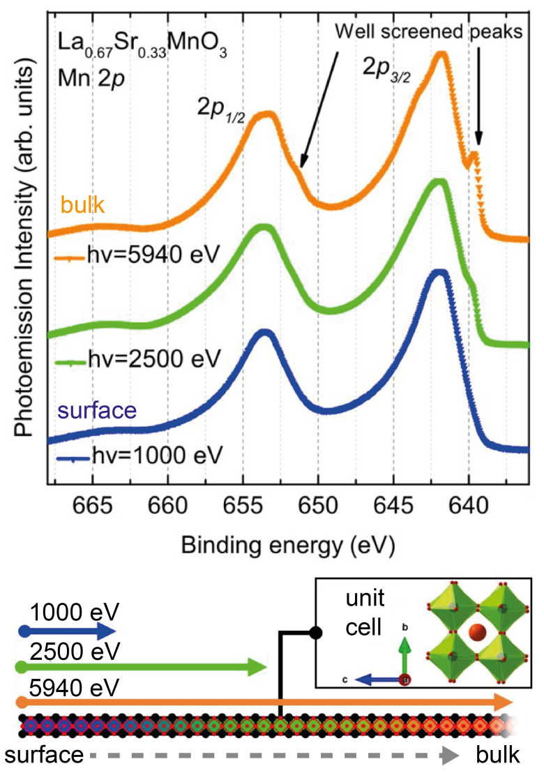
Since the photoelectrons have to exit the sample through its surface in order to be detected, one might expect that the technique would be most sensitive to electron states near the surface of the sample. This is generally true, but by tuning the energy of the incoming X-ray beam one can vary the characteristic length scale which is being probed in the measurement. With higher energy X-rays, the ejected photoelectrons also have higher energy, and can exit the sample from deeper inside the material.
To find out more about the I09 beamline, or to discuss potential applications, please contact Principal Beamline Scientist Dr Tien-Lin Lee: [email protected].
Pincelli T et al. Quantifying the critical thickness of electron hybridization in spintronics materials. Nature Communications (2017) DOI: 10.1038/ncomms16051.

Diamond Light Source is the UK's national synchrotron science facility, located at the Harwell Science and Innovation Campus in Oxfordshire.
Diamond Light Source Ltd
Diamond House
Harwell Science & Innovation Campus
Didcot
Oxfordshire
OX11 0DE
Copyright © Diamond Light Source. Diamond Light Source® and the Diamond logo are registered trademarks of Diamond Light Source Ltd
Registered in England and Wales at Diamond House, Harwell Science and Innovation Campus, Didcot, Oxfordshire, OX11 0DE, United Kingdom. Company number: 4375679. VAT number: 287 461 957. Economic Operators Registration and Identification (EORI) number: GB287461957003.