- Science
- Research
- Science Highlights
- 2015
- Surfaces-and-Interfaces
- Electronic-structure-and-spin-valley-layer-coupling-in-the-strong-spin-orbit-semiconductor-WSe2
 | ||
Electronic structure and spin-valley-layer coupling in the strong spin-orbit semiconductor WSe2 |
Spintronics is a novel field of electronics that exploits electron spins with the hope of developing faster, more energy-efficient devices. Materials with a strong coupling between the spin and orbital motion of an electron, so-called spin-orbit coupling, represent a promising route to achieve such aims. A compound expected to have strong spin-orbit coupling, the layered semi-conductor WSe2, was previously studied at the MAX-lab synchrotron using spin- and angle-resolved photoemission spectroscopy. The results indicated that the material has electronic states where the electrons are spin-polarised, effectively aligned in one direction of the substance. This is contrary to what would be expected from the symmetry of the material. The bulk structure was investigated further to determine the origins of these surprising results by using the Angle-Resolved Photoemission Spectroscopy (ARPES) beamline (I05) at Diamond Light Source. ARPES measurements over a wide photon energy range enabled detailed imaging of the electronic band dispersions in three dimensions, and were in excellent agreement with theoretical calculations, providing confirmation that the electronic structure of the bulk material was being observed. The key finding from the study shows that this non-magnetic substance has spin-polarised states arising from its layered structure. Each of the individual layers that make up the crystal lacks inversion symmetry, which permits the aligned spin-polarised states in each separate layer. However, these layers are stacked with 180° rotation between neighbouring layers, so that the spin polarisation is opposite in adjacent layers, restoring the overall symmetry of the system. This opens a wealth of opportunities in spintronics and new materials for highly efficient computations.
Beamline I05 Scientific Highlight
The effects of strong spin-orbit coupling in solids have been brought to particular prominence in recent years through the discovery of topological insulators1 and giant Rashba effects2. Both systems support the existence of strongly spin-polarised electronic states, which could in principle be harnessed to allow the electrical control of electron spins in a device. There are hopes this will usher in new schemes of energy-efficient electronics, termed spintronics. While spin-orbit coupling is certainly necessary to stabilise such spin-polarised states in the absence of magnetism, it is also known not to be sufficient. A second crucial ingredient is the breaking of structural inversion symmetry.
In this work, the influence of strong spin-orbit coupling on the electronic structure of the semiconductor WSe2 is investigated. Using photon energydependent ARPES measurements, strong signatures of spin-orbit coupling are revealed. A dichotomy between two- and three- dimensional electronic states is found at different momentum-space locations, mediated partly by spin-orbit coupling. Where these intersect, the opening of pronounced hybridisation gaps is revealed. More surprising, where the electronic wavefunctions become strongly confined in individual layers of the crystal structure, additional spin-resolved ARPES measurements reveal the emergence of strongly spin- Surfaces and Interfaces Village Beamline I05 polarised bulk electronic states, despite the bulk crystal structure remaining inversion symmetric.
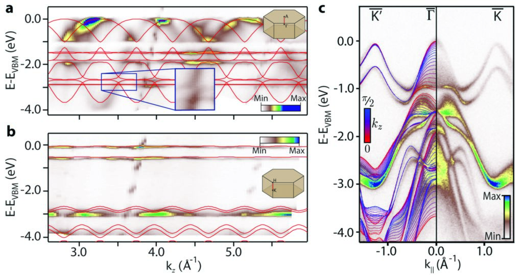
Figure 1: Bulk electronic structure of WSe2 measured by photon-energy dependent ARPES along the (a) G- A and (b) K-H directions of the threedimensional Brillouin zone (shown inset), and (c) along the Κ' - Γ - Κ direction of the surface Brillouin zone. In all cases, the electronic band dispersions calculated by density-functional theory are overlaid (solid lines). Adapted from Nature Physics 10 (2014) 835.
The three-dimensional electronic structure of WSe2 (Fig. 1) is measured using photon-energy-dependent ARPES at Diamond’s I05 beamline. Measurements performed over a wide photon energy range from 20 to 130 eV were used to extract the electronic dispersion relations along the out-ofplane direction (kz), shown in Fig. 1a,b. Starting from the zone centre Γ point, a strong out-of-plane dispersion is found, characteristic of a three-dimensional bulk solid (Fig. 1a). Where several states intersect, anti-crossing gaps can be clearly observed. This is a direct indication of the prevalent role of spin-orbit coupling in this material. Neglecting such hybridisation gaps, however, a broad electronic bandwidth of over 4 eV is evident, reflecting the spatilallyextended 5d orbitals that make up these states. The situation is very different at the corners of the Brillouin zone (Fig. 1b). The upper valence band states are almost dispersionless along the K-H direction. This indicates two-dimensional electronic states, whose wavefunctions must therefore be strongly confined in individual planes of the crystal which stack along the z-direction of this highlylayered material. The splitting of ~0.5 eV between the two upper valence band states is again driven by strong spin-orbit interactions, which act to stabilise the highly two-dimensional nature of these electronic bands around Κ3. This measured electronic structure is in excellent agreement with that calculated for an ideal bulk WSe2 crystal by density-functional theory, both along the kz-direction and throughout the surface Brillouin zone (Fig. 1c), confirming the bulk origin of these states.
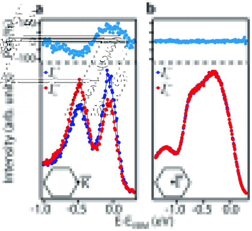
Figure 2: Spin-resolved ARPES measurements of the upper valence bands at the (a) Κ and (b) Γ points of the surface Brillouin zone, measured using a photon energy of 25 eV. The measured intensities on the out-of-plane detectors in the Mott scattering chamber are shown, together with a corresponding extracted spin polarisation correcting for the finite efficiency of Mott detectors and geometric factors. Adapted from Nature Physics 10 (2014) 835.
Intriguingly, spin-resolved ARPES measurements performed at MAXlab's I3 beamline revealed the two-dimensional states at Κ to be almost 100% spin-polarised, an effect which completely disappears for the threedimensional states near Γ. This seems surprising, as the bulk crystal structure of WSe2 is centrosymmetric, lacking the broken inversion symmetry that is conventionally assumed a prerequisite for stabilising spin-polarised electronic states in the absence of magnetism.
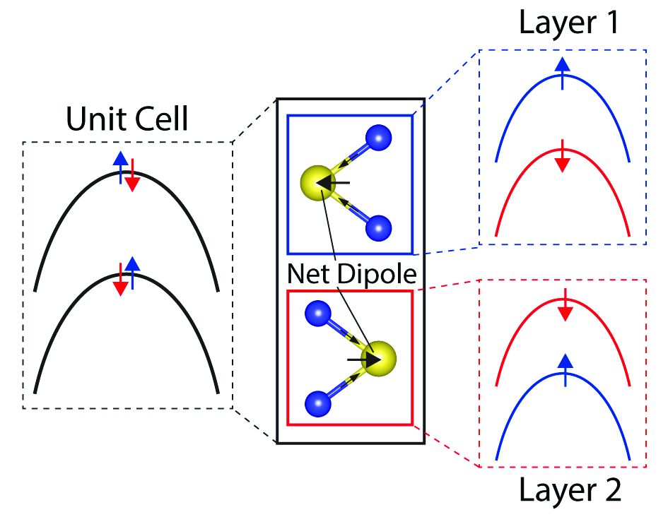
Figure 3: Structural model of the WSe2 unit cell, with a schematic decomposition of the valence
band states at Κ showing how strong layer-dependent spin polarisations develop, yet the
total electronic structure remains spin degenerate as required by symmetry.
An explanation can be found from a more detailed look at the crystal structure of this compound (Fig. 3). The unit cell is composed of two Se-WSe layers, stacked along the z-axis, with a relative rotation of 180° between neighbouring layers. Each layer lacks a centre of inversion when considered in isolation, but this so-called ‘AB’ stacking of neighbouring layers restores inversion symmetry for the bulk crystal as a whole. As discussed above, around the Brillouin zone corners, the electronic states are very two-dimensional, meaning that the electronic wavefunctions are confined within a single layer. The strongly broken inversion symmetry within such individual layers allows the electronic states to develop a large spin polarisation, whose sign is reversed in neighbouring layers due to their 180° relative rotation (Fig. 3). This is again fully reproduced by the study's first-principles calculation, and ensures that, taken together, the electronic structure arising from both layers of the unit cell remains spin-degenerate as required by the centrosymmetric nature of the crystal’s space group. Nonetheless, locally, strong spin polarisations can develop. Moreover, the spin direction is also reversed at opposite corners of the Brillouin zone as a consequence of time-reversal symmetry, leading to a spin texture that is strongly modulated in both real and momentum space. Physically, this represents a strong locking between the spin, a layer pseudospin, and a so-called valley pseudospin in these compounds4.
More generally, the observation of a locally well-defined but exactly compensated spin polarisation in a non-magnetic, centrosymmetric material can be viewed as a new ‘hidden’ form of spin polarisation, mediated by a lack of inversion symmetry of constituent structural units where the electronic states are localised5. Harnessing control over this promises exciting new possibilities for the creation of optimised spintronic materials.
Source publication:
Riley, J. M., Mazzola, F., Dendzik, M., Michiardi, M., Takayama, T., Bawden, L., Granerod, C., Leandersson, M., Balasubramanian, T., Hoesch, M., Kim, T. K., Takagi, H., Meevasana, W., Hofmann, P., Bahramy, M. S., Wells, J. W. & King, P. D. C. Direct observation of spin-polarized bulk bands in an inversion-symmetric semiconductor. Nature Physics 10, 835-839, doi:10.1038/nphys3105 (2014).
References:
1. Hasan, M. Z. & Kane, C. L. Colloquium: Topological insulators. Reviews of Modern Physics 82, 3045-3067, doi:10.1103/RevModPhys.82.3045 (2010).
2. Ishizaka, K. et al. Giant Rashba-type spin splitting in bulk BiTeI. Nature Materials 10, 521-526, doi:10.1038/nmat3051 (2011).
3. Gong, Z. et al. Magnetoelectric effects and valley-controlled spin quantum gates in transition metal dichalcogenide bilayers. Nature Communications 4, doi:10.1038/ncomms3053 (2013).
4. Xu, X., Yao, W., Xiao, D. & Heinz, T. F. Spin and pseudospins in layered transition metal dichalcogenides. Nature Physics 10, 343-350, doi:10.1038/nphys2942 (2014). 5. Zhang, X., Liu, Q., Luo, J.-W., Freeman, A. J. & Zunger, A. Hidden spin polarization in inversion-symmetric bulk crystals. Nature Physics 10, 387- 393, doi:10.1038/nphys2933 (2014).
Funding acknowledgements:
We acknowledge Diamond for experimental beamtime on I05 under awards SI9427 and SI9500, and MAXlab for beamtime under award 20140014. We gratefully acknowledge support from the Royal Society, UK, the Engineering and Physical Sciences Research Council, UK, the Ministry of Education, Culture, Sports, Science and Technology (MEXT) of Japan, the VILLUM foundation, the Calipso program, TRF-SUT Grant RSA5680052 and NANOTEC, Thailand through the CoE Network.
Corresponding author:
Dr Phil King, University of St Andrews, [email protected]

Diamond Light Source is the UK's national synchrotron science facility, located at the Harwell Science and Innovation Campus in Oxfordshire.
Diamond Light Source Ltd
Diamond House
Harwell Science & Innovation Campus
Didcot
Oxfordshire
OX11 0DE
Copyright © Diamond Light Source. Diamond Light Source® and the Diamond logo are registered trademarks of Diamond Light Source Ltd
Registered in England and Wales at Diamond House, Harwell Science and Innovation Campus, Didcot, Oxfordshire, OX11 0DE, United Kingdom. Company number: 4375679. VAT number: 287 461 957. Economic Operators Registration and Identification (EORI) number: GB287461957003.