High-energy transmission Laue (HETL) diffraction: a tool for mapping grain-level orientation and strain in thicker metallic polycrystals
Feb 20, 2013
Feb 20, 2013
Micro-beam Laue diffraction is a versatile probe for orientation and elastic strain in individual grains of metallic polycrystals. It can help elucidate the dependence of macroscopic material behaviour (deformation response, fatigue, fracture etc.) on microstructure, defect population, macro- to microscopic load redistribution, etc. Furthermore, it can provide quantitative validation for the crystal plasticity models used to study structural engineering alloys. The application of micro-beam Laue diffraction to real-life engineering components is limited by the absorption of the probing beam. To improve penetration into thicker samples we developed a high-energy transmission Laue (HETL) micro-beam diffraction setup on I12. The use of higher photon energies (50 – 150 keV) permits measurements in several-millimetre-thick polycrystalline samples. We established two different approaches to extend this method and allow resolution in three dimensions. The first approach relies on the application of tomographic reconstruction principles to orientation-specific scattered intensity. The second uses wire scans and triangulation to determine the volume of origin of each scattered contribution recorded on the detector.
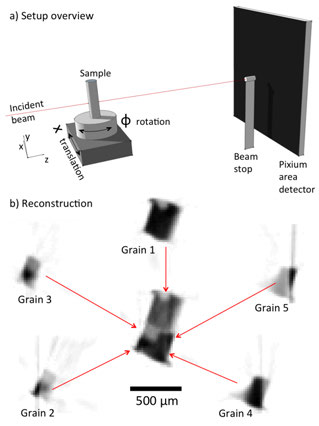 |
| Figure 1: Laue Orientation Tomography (LOT). a) Schematic of the experimental setup. b) Reconstruction of 5 grains in the cross-section of a polycrystalline nickel sample. |
For safety-critical aerospace applications, the ability to obtain accurate predictions of the grain-level response to deformation of polycrystalline alloys is essential. This is particularly the case since material failure is governed by 'weakest link' type mechanisms such as grain boundary creep and cracking, void nucleation, etc. that strongly depend on local inter- and intra-granular interactions and on the partitioning of macroscopic loading at the micro-scale. Computationally these phenomena can be studied by crystal plasticity simulations that take into account local morphology, evolution of crystal slip, lattice rotation and dislocation density1,2. For model calibration and validation, experimental measurements at the same (micro-) scale are essential. Micro-beam Laue synchrotron X-ray diffraction is ideally suited to this purpose. Conventionally, a polychromatic, micro-focussed X-ray beam probe (5-25 keV) is used to illuminate intra-granular scattering volumes. The resulting diffraction patterns consist of a number of Laue spots and are recorded on an area detector positioned in reflection geometry. By indexing the spots and refining their positions, lattice orientation and elastic strain in the scattering volume can be computed3,4. Orientation spread in the illuminated volume causes streaking of reflections that can be interpreted in terms of the underlying dislocation structure and active slip system(s)5.
The shallow penetration of the probing beam (~70 μm in nickel) precludes the application of micro-beam Laue diffraction to the study of deformation in the bulk of real-life engineering components. To increase penetration to several millimetres, we extended the technique to significantly higher photon energies (50 to 150 keV). Transmission geometry is the natural choice since Braggs’ law dictates that at higher photon energies, the stronger, lower order reflections are forward scattered6. We used this new technique to study the evolution of lattice orientation and strain in individual grains of polycrystalline nickel samples during in-situ deformation. The results highlighted that, even for uniform macroscopic loading, significant heterogeneities exist at the grain-scale. Furthermore the local stress state is strongly influenced by the morphology of the grain neighbourhood.
|
| Figure 2: High Energy Differential Aperture X-ray Microscopy (HEDAXM). a) Schematic of the experimental setup. b) Experimental Laue pattern of three-layered silicon wafer sample. c)-e) Reconstructed Laue patterns from each of the three silicon wafer layers. |
At beamline I12 we developed two novel techniques to extend HETL to 3D grain-level resolution. The first, Laue Orientation Tomography (LOT), relies on the application of tomographic reconstruction principles to orientation-specific scattered intensity. The sample is mounted in transmission geometry (Fig. 1a.). Laue patterns are collected at x-positions covering the entire width of the sample for 91 φ-rotations between 0° and 180°. Indexation of the Laue patterns acts as an orientation-sensitive filter. Similar to absorption tomography, lattice-orientation-specific sinograms ('origrams') are then established as functions of x and φ, considering only the scattered intensity I12that corresponds to a certain orientation. The shapes of individual grains in the illuminated sample slice are reconstructed by inverting these 'origrams' using filtered back projection algorithms. Fig. 1b. shows five grains present in the slice of a polycrystalline nickel sample reconstructed on I12. To map the full 3D microstructure, slices at different heights of the sample are reconstructed. Further work is under way to obtain maps of intra-granular mis-orientation within individual crystallites.
The second technique, High Energy Differential Aperture X-ray Microscopy (HEDAXM), is an extension of the corresponding low energy technique7. Tungsten wires are scanned across the scattered beams immediately downstream of the sample (Fig. 2a.). When a given reflection is obscured by a scanning wire we triangulate from the reflection position on the detector, via the wire, to the incident beam. Hence the through-thickness position of the coherently scattering volume that gives rise to the reflection can be determined. On I12 we studied a three-layer silicon wafer sample as a proof of principle. Fig. 2b., shows the complete diffraction pattern arising from this sample. Using HEDAXM we successfully separated this pattern into the individual contribution from each layer (Fig. 2c-e.).
These successful first results demonstrate the promise of LOT and HEDAXM for the 3D mapping of microstructure, lattice orientation and elastic strain in individual grains of polycrystalline engineering samples.
Hofmann, F., Abbey, B., Connor, L., Baimpas, N., Song, X., Keegan, S. & Korsunsky, A.M. Imaging of grain-level orientation and strain in thicker metallic polycrystals by high energy transmission micro-beam Laue (HETL) diffraction techniques. Int. J. Mat. Res. 103, 192-199 (2012)
Hofmann, F., Song, X., Abbey, B., Jun, T.-S., Korsunsky, A. M. High-energy transmission Laue micro-beam X-ray diffraction: a probe for intra-granular lattice orientation and elastic strain in thicker samples, J. Sync. Rad. 19, 3 (2012)

Diamond Light Source is the UK's national synchrotron science facility, located at the Harwell Science and Innovation Campus in Oxfordshire.
Diamond Light Source Ltd
Diamond House
Harwell Science & Innovation Campus
Didcot
Oxfordshire
OX11 0DE
Copyright © Diamond Light Source. Diamond Light Source® and the Diamond logo are registered trademarks of Diamond Light Source Ltd
Registered in England and Wales at Diamond House, Harwell Science and Innovation Campus, Didcot, Oxfordshire, OX11 0DE, United Kingdom. Company number: 4375679. VAT number: 287 461 957. Economic Operators Registration and Identification (EORI) number: GB287461957003.