A novel dilute magnetic semiconductor
Sep 23, 2010
Sep 23, 2010
The vast majority of the electronic devices today are based on silicon technology and their performance and operation depend on the movement and mobility of electronic charge. This mode of operation sets the limits on power consumption, operation speed and results in potential device overheating, particularly at fast switching speeds. At the same time, it is well-known that electrons also possess a spin and the idea of manipulating this property led to a relatively new field of
research - spintronics.
One of the goals of spintronics is to combine the magnetic memory storage capabilities of a hard disc with the electronics of a microprocessor in a single chip, leading to smaller and faster devices that resolve the issues mentioned above and use much less power. The group of dilute semiconductors with Curie temperatures well in excess of room temperature is one of the most interesting magnetic materials to emerge in the last few years. While the III-V and oxide-based ferromagnetic semiconductors have been well explored the study of magnetism in the technologically important group IV semiconductors has somewhat lagged behind. In earlier studies of Mn-implanted Si [1, 2] it was not clear whether the magnetism was intrinsic or due to new phase and/or cluster formation because of high temperature processing.
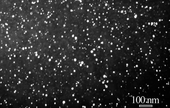
Figure 1: TEM image of MnxSiy nanoclusters in a Si matrix.
We have performed EXAFS studies and used beamline I18’s microfocus capabilities to map Mn distribution in dilute magnetic semiconductor (Mn-doped Si) in order to shed light on the question of possible origins of magnetism in Mn-implanted Si layers. Mapping has indicated the uniform distribution of Mn in our samples and confirms TEM results (Fig. 1). This was found to be true for the samples annealed after ion implantation as well as those not subject to the annealing. X-ray absorption spectra of the Mn doped Si samples were collected in the vicinity of the Mn absorption K-edge (6539 eV, Fig. 2). EXAFS spectra of as-prepared and annealed samples were found to be similar and did not change significantly within the studied concentration range of Mn (3%-5%). The near edge region (between 6530 eV and 6630 eV) of the x-ray absorption spectrum was found to be similar to the simulated spectrum of MnSi B20-type structure (Fig. 3). Specifically, close inspection reveals three features in the region below the maximum signal value (so-called “white line”). These features are particularly obvious in the first derivative of the signal. One can clearly see at least two distinct coordination shells of atoms around Mn in the magnitude of the Fourier-Transform of the k2-weighted absorption fine structures extracted above the Mn edge. Further analysis revealed that the first shell is definitely composed of Si atoms more than 4 in number. Therefore, we can conclude that Si layer does not contain a detectable amount of Mn clusters. This may suggest interstitial Mn in the Si lattice, but we found that the second shell is composed of Mn atoms rather than Si. Multiple scattering EXAFS analysis (with a path length of up to 15 Å, with up to 3 atoms in the path, within a cluster based on MnSi B20 structure) produced the following results for two shell model around Mn (where R – distance, N – number of atoms, σ2 – Debye-Waller factor): R(Mn-Si) = 2.38(1) Å, N(Si) =7(1), σ2(Mn-Si) = 0.017(4) Å2, R(Mn-Mn) = 2.95(1) Å, N(Mn)= 2.5(9), σ2(Mn-Mn) = 0.005(1) Å2. Here numbers in parenthesis are the corresponding errors in the last digits. The Debye-Waller factor (mean-square relative displacement of atoms) is rather large for the first peak and this is likely to be due to the presence of more than one shell under the peak, but further detailed analysis is limited by the available data range. The interesting result here is that the second shell consists of only Mn atoms. In fact, we found that it was impossible to obtain a satisfactory fit with any other configuration (e. g. Si atoms in second shell).
Figure 2: X-ray absorption fine structure signal at Mn K edge (top, collected at T = 80 K) and its magnitude of Fourier transform (bottom, dotted line) together with the calculated signal (solid line).
Figure 3: XANES part of the x-ray absorption spectra together with simulated spectrum for MnSi B20 structure. Inset shows first derivatives for each spectrum, arrows mark features corresponding to the region below the “white line’’.
Thus, the main finding of this work is that we observe neither formation of Mn clusters nor isolated Mn impurities as a result of ion implantation of Si wafers. Instead, results of analysis of EXAFS data confirm that the clusters of MnSi are formed and that these clusters are stable under annealing. EXAFS data suggest that these clusters are likely to be similar to B20 type and/or to MnSi1.7 structures. These clusters are also under tensile strain from the host Si matrix (as can be concluded from increased Mn-Mn distances and a consequence of lattice mismatch between Si (a = 5.431 Å) and MnSi (a= 4.558 Å)) which effectively results in negative pressure exerted on the clusters. We believe that this as well as the nanocrystalline nature of the clusters are responsible for increase of Curie temperature above room temperature. However, while some information exists on pressure dependence of magnetic properties on bulk MnSi with B20 type structure, there is no information as to whether this dependency will hold for MnSi nano crystals. There is also little information on magnetic properties of MnSi1.7. We believe that further efforts should be directed towards conducting XMCD experiments at Mn L-edges in Mn-implanted Si. Such experiments would clarify the role of Mn in magnetic properties of Mn-implanted Si.
References
[1] F. M. Zhang, X. C. Liu, J. Gao, X. S. Wu, Y. W. Du, H. Zhu, J. Q. Xiao, and P. Chen, Appl. Phys. Lett. 85, 786 (2004).
[2] M. Bolduc, C. Awo-Affouda, A. Stollenwerk, M. B. Huang, F. G. Ramos, G. Agnello, and V. P. LaBella, Phys. Rev. B, 71,
033302, (2005).
Principal Publications and Authors
A. Orlov, A. Sapelkin, A. F. Granovsky, Structure, electrical and magnetic properties, and the origin of the room temperature ferromagnetism in Mn-implanted Si, Journal of Experimental and Thoretical Physics, Vol: 109:602-608, (2009). DOI: 10.1134/S1063776109100069
Funding Acknowledgement
Russian Foundation for Basic Research Grant number 07-02-00327.

Diamond Light Source is the UK's national synchrotron science facility, located at the Harwell Science and Innovation Campus in Oxfordshire.
Diamond Light Source Ltd
Diamond House
Harwell Science & Innovation Campus
Didcot
Oxfordshire
OX11 0DE
Copyright © Diamond Light Source. Diamond Light Source® and the Diamond logo are registered trademarks of Diamond Light Source Ltd
Registered in England and Wales at Diamond House, Harwell Science and Innovation Campus, Didcot, Oxfordshire, OX11 0DE, United Kingdom. Company number: 4375679. VAT number: 287 461 957. Economic Operators Registration and Identification (EORI) number: GB287461957003.