
Keep up to date with the latest research and developments from Diamond. Sign up for news on our scientific output, facility updates and plans for the future.
Angle-Resolved PhotoEmission Spectroscopy (ARPES) is a standard tool for the study of the electronic structure of solids and their surfaces. It is applied to semiconductors and metals for the study of strongly correlated electron systems, the physics of superconductors, charge density waves, and many other topics in material science.
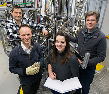
First users on the nano-ARPES end station with the I05 team. L-R: Pavel Dudin (I05), Neil Wilson and Natalie Teutsch (both University of Warwick), and I05’sPrincipal Beamline Scientist Dr Moritz Hoesch.
Many materials relevant for traditional ARPES are intrinsically inhomogeneous at the sub-micron scale. New applications become possible with the new nano-focusing branch using Scanning Photoemission Spectromicroscopy (nano-ARPES), such as in operando studies of micro-electronic thin film devices. With a light spot well below 1 micron, this technique gives the required spatial resolution.
The nano-ARPES branchline on I05 took first light in November 2014. Currently user experiments alternate with intense optimisation work. User proposal submission has been open since 2016.
The nano-ARPES end station complements the current operational I05 end station that delivers classical ARPES with high resolution in energy and momentum. The surface-sensitive character of ARPES microscopy makes it complementary to many other surfacesensitive techniques, like Low-Energy or PhotoEmission Electron Microscopy (LEEM or PEEM) on the Nanoscience beamline (I06).
To find out more about nano-ARPES on I05, contact the Principal Beamline Scientist, Dr Moritz Hoesch: [email protected]
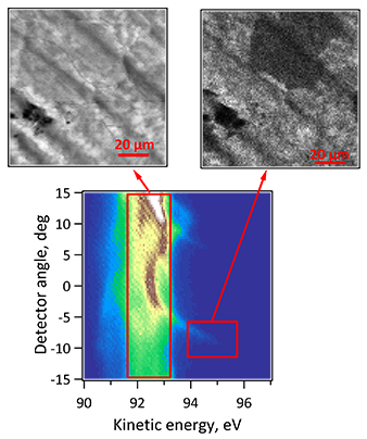
Micro-spot dispersion of electrons in graphene on a Cu foil (bottom). Images are acquired with different contrasts (top, left and right) depending on the energyangle region (marked with red rectangles), corresponding to all Cu d-electrons and graphene sp-electrons in a specific orientation.
“I08 gives us unique data on distributions and speciations on light elements that are otherwise not feasible. The ability to map at this resolution, allows us to determine the nature of heterogeneities in our complex environmental samples.”
Professor Liane G. Benning, University of Leeds and German Research Centre for Geosciences

Diamond Light Source is the UK's national synchrotron science facility, located at the Harwell Science and Innovation Campus in Oxfordshire.
Copyright © 2022 Diamond Light Source
Diamond Light Source Ltd
Diamond House
Harwell Science & Innovation Campus
Didcot
Oxfordshire
OX11 0DE
Diamond Light Source® and the Diamond logo are registered trademarks of Diamond Light Source Ltd
Registered in England and Wales at Diamond House, Harwell Science and Innovation Campus, Didcot, Oxfordshire, OX11 0DE, United Kingdom. Company number: 4375679. VAT number: 287 461 957. Economic Operators Registration and Identification (EORI) number: GB287461957003.

 A brighter light for science