X-rays help to unravel the structure and orientation of semiconductive porous ultrathin films
Jul 30, 2019
Jul 30, 2019
MOFs combine the extended structure and high crystallinity of inorganic solids with the synthetic versatility, and easy processability and mechanical flexibility, of organic materials. Furthermore, their porous structures offer the possibility of indirectly manipulating their properties by infiltration with active guests. Nevertheless, most consolidated applications employ MOFs as electronically innocent frameworks, as most of them are electrical insulators. However, the appearance in recent years of various examples of conductive MOFs has opened a pathway of integration of MOF materials as active elements in electronic devices1,2. A fundamental difference from other applications is the fact that a very small amount of material is needed for electronic devices, in other words, they have to be prepared or processed as thin films. In this regard, this constitutes the very first step in device integration; materials must be carefully processed to achieve nanometric thicknesses with exquisite control over several factors that play an important role in the device performance, such as film thickness, substrate coverage, homogeneity, roughness, crystallinity, and crystalline orientation with respect to the substrate. Controlling these parameters is necessary so that the designer properties of the original bulk material are equivalent in its nanostructured form. However, this nanostructuring also carries with it a challenge with regards to their characterisation.
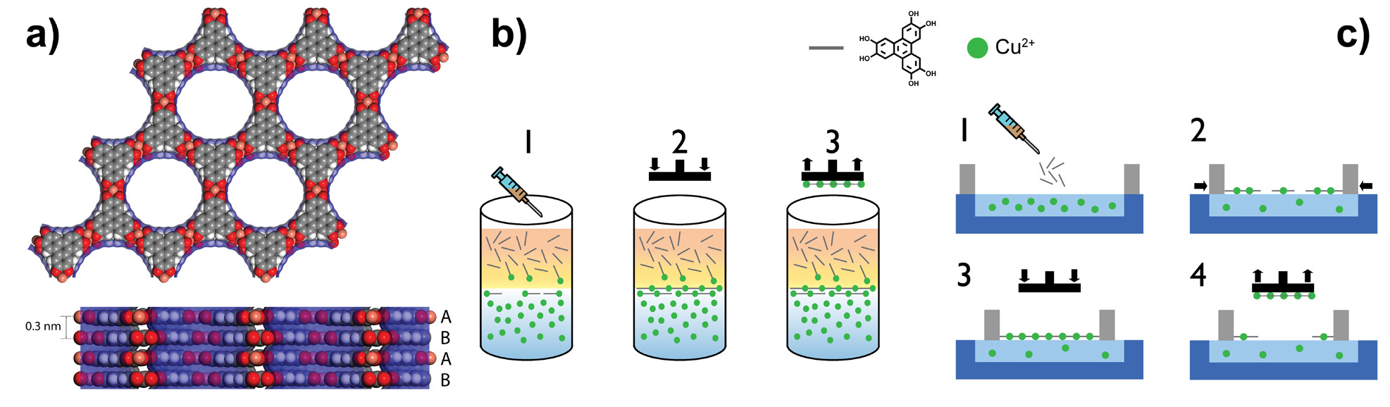
After our first work, which involved the fabrication of the electronic properties of ultrathin films of a moderately conductive and non-intrinsically porous MOF3, we moved on to apply the acquired nanofabrication expertise to an intrinsically conductive and porous system. For that purpose, we chose a previously reported material: Cu-CAT-14, a highly conductive MOF composed of hexagonal layers of 2, 3, 6, 7, 10, 11-hexahydroxytriphenylene (HHTP) ligands in the semiquinone form and square planar Cu2+ ions (Fig. 1a). In order to produce ultrathin films of Cu-CAT-1, we employed two complementary deposition strategies, a facile and versatile liquid–liquid (LL) method (Fig. 1b), and a more demanding but highly controllable Langmuir-Blodget (LB) procedure (Fig. 1c). In both routines, the Cu-CAT-1 ultrathin film is synthesised at the interphase between two immiscible liquid mediums, and then transferred to a solid substrate. We used spectroscopic techniques like infrared reflectance absorption spectroscopy (IRRAS), UV-vis, or X-ray photoelectron spectroscopy (XPS) to confirm the successful formation and transfer of Cu-CAT-1 ultrathin films onto substrates, as well as microscopic ones such as optical microscopy, atomic force microscopy (AFM), and scanning electron microscopy (SEM) to assess the films’ roughness, thickness and morphology. However, structural studies key to confirming their crystallinity and preferential orientation long-range order were still missing. Thus, we performed 2D grazing incidence X-ray diffraction (2D-GIXRD) at beamline I07.
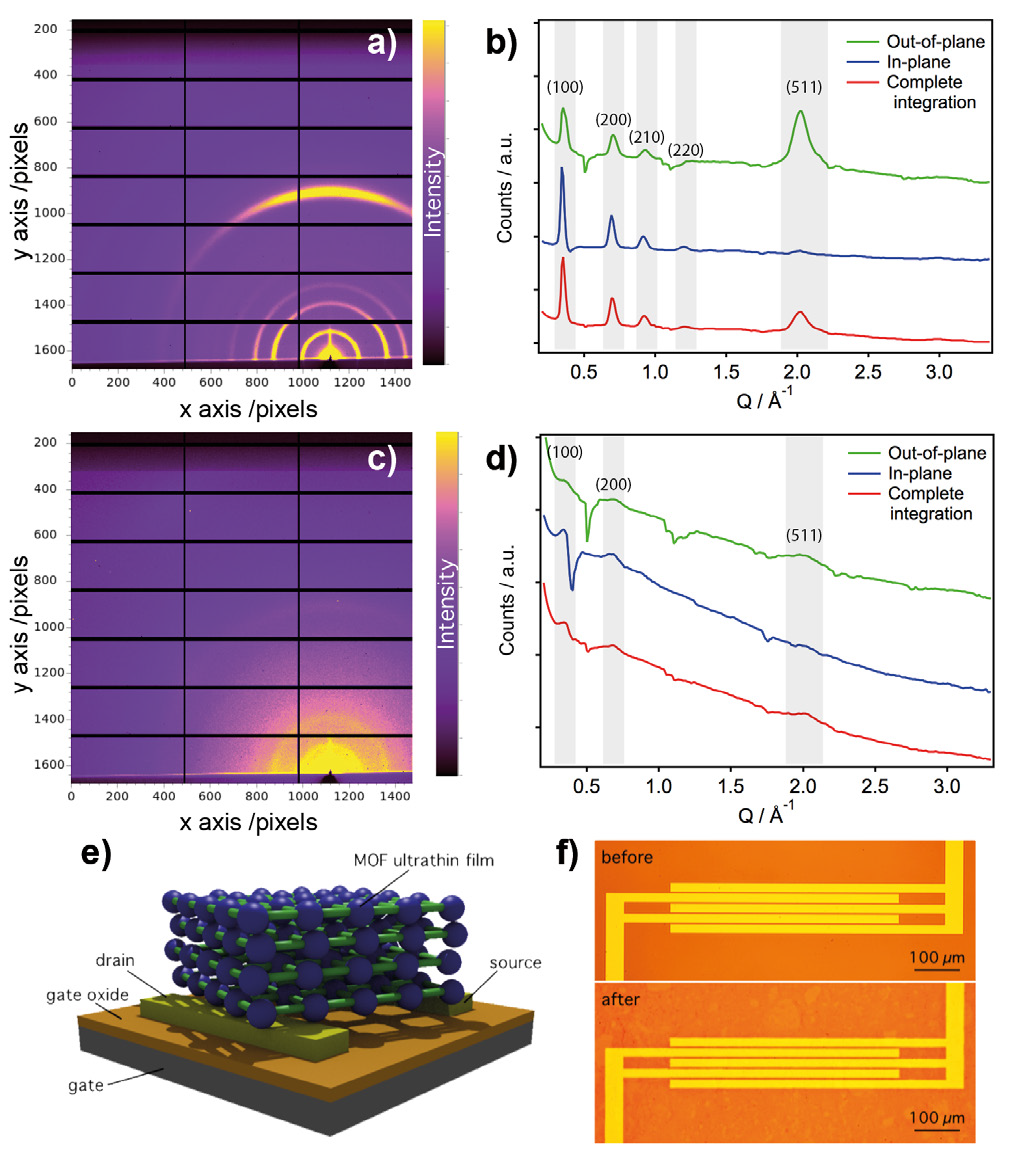
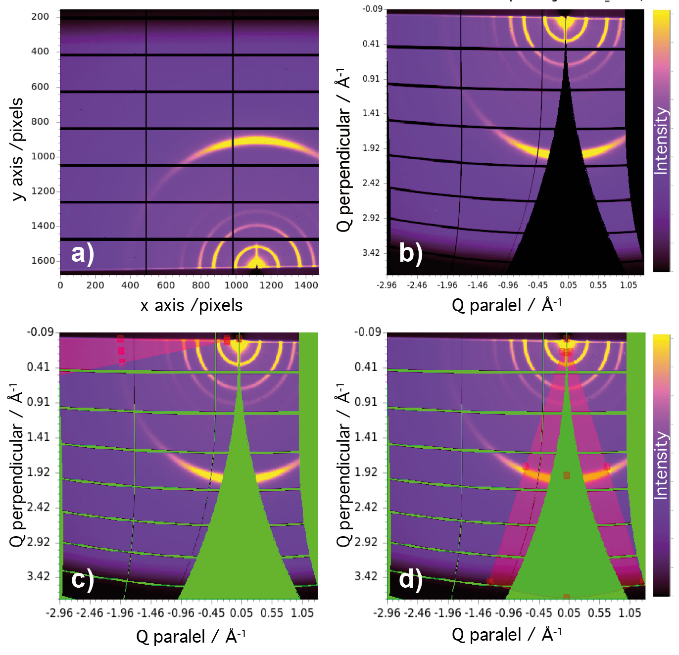
Cu-CAT-1 ultrathin films fabricated onto Si/SiO2 substrates, with both LL and LB procedures, were placed into a closed cell mounted on a multiaxis diffractometer, and measured under a continuous helium flow to minimise beam damage. We then collected 2D-GIXRD single shot images at room temperature using a Pilatus 2M area detector with a wavelength of 0.85 Å (beam energy of 14.53 keV), a sample-to-detector distance of 456 mm, and an incidence angle of 0.1º above the critical angle. Next, the resulting real space images were processed into Q-space images using the DAWN software, and complete in-plane and out-of-plane profiles were extracted by simple sector integration of the Q-space images (Fig. 2). As seen in Fig. 3, the complete 2D-GIXRD pattern for both LL and LB ultrathin films showed the characteristic peaks of Cu-CAT-1. Additionally, the higher intensity of the (001) peak in the out-of-plane XRD profiles with respect to the in-plane diffractograms indicates that the films are preferentially oriented with the hexagonal sheets (ab plane) laying parallel to the surface of the substrate. The difference in intensity between LL and LB diffractograms can be ascribed to the disparity in the thickness of the films analysed (~20-70 nm for LL vs. ~20 nm for LB).
References:

Diamond Light Source is the UK's national synchrotron science facility, located at the Harwell Science and Innovation Campus in Oxfordshire.
Diamond Light Source Ltd
Diamond House
Harwell Science & Innovation Campus
Didcot
Oxfordshire
OX11 0DE
Copyright © Diamond Light Source. Diamond Light Source® and the Diamond logo are registered trademarks of Diamond Light Source Ltd
Registered in England and Wales at Diamond House, Harwell Science and Innovation Campus, Didcot, Oxfordshire, OX11 0DE, United Kingdom. Company number: 4375679. VAT number: 287 461 957. Economic Operators Registration and Identification (EORI) number: GB287461957003.