Chris Nicklin, Village Coordinator
The Surfaces and Interfaces village comprises six different beamlines, five of which are in operation and one is currently under development. All six beamlines support investigations into the physical or electronic structures of interfaces and surfaces, with users having the ability to study core and weakly bound electrons, magnetism, atomic and nanostructure and to image with chemical sensitivity. Together the village’s beamlines provide a range of techniques including X-ray Photoelectron Spectroscopy (XPS), X-ray Absorption Spectroscopy (XAS), X-ray diffraction (XRD), Photo Emission Electron Microscopy and X-ray Magnetic Circular or Linear Dichroism (XMLD or XMCD). A choice of sample environments and X-ray energies opens up the village to a range of scientific studies, with strengths including the study of multiferroics, superconducting materials, topological insulators and photovoltaics.
A cuprate-like pseudogap in lightly doped Sr2IrO4
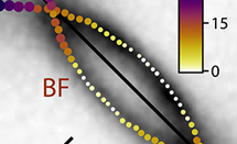 Mott insulators are a class of materials that should be conductors, according to conventional band theories, but which are insulators particularly at low temperatures. First described in 1937, the proposed explanation was that this anomaly is due to electron electron interactions not considered in conventional band theories. Mott insulators are of interest because some of them, the layered copper oxides, or ‘cuprates’, become superconducting up to high critical temperature when their chemical composition is modified slightly to dope them with additional valence electrons (or ‘holes’). Read More
Monitoring the bonding of CO molecules on a single Pd nanoparticle
 Metal nanoparticles form the basis of heterogeneous catalysts because they offer a bigger surface area compared to bulk metal, which increases catalytic activity. To optimise performance, it is important to know how molecules adsorb to them compared to single crystals. Palladium (Pd) nanoparticles supported on a substrate of titanium dioxide, TiO2(110), were selected as the test system because it is familiar and well understood. Read More
Competitive growth of fullerene crystals in polymer fullerene thin-films
 The performance of composite fullerene/polymer films, which are potential candidates for the new generation of solar cell technology, is hindered by the growth of large (microscale) crystals. This study of model layered materials shows that crystal growth in a fullerene layer can be carefully controlled by the presence of an adjacent polystyrene (PS) polymer layer. In silicon-supported samples a thinner PS polymer layer promotes the growth of smaller-sized nanocrystals in the fullerene layer, [6,6]-phenyl C61-butyric acid methyl ester (PCBM), which in turn impedes the growth rate of the larger microcrystals. By using a combination of Grazing-Incidence X-ray Diffraction (GIXD) provided by the Surface and Interface Diffraction beamline (I07) and optical microscopy, the relationship between polymer thickness and competitive crystallisation behaviour was examined. Read More
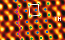
Gauging the interaction of graphene with its substrate
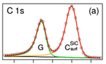 Graphene is a single layer hexagonal lattice form of carbon known for its remarkable electronic and structural properties. Applications include transistors in nanoscale devices, fuel cells, lithium-ion batteries, and high strength composite materials. Graphene in electronics is almost always supported by another material and to preserve its electronic properties, the interaction with the associated substrate has to be as small as possible. The precise material properties of graphene depend on the growth conditions on the substrate and its interaction with the substrate. Here, a supported form of graphene termed ‘hydrogen intercalated quasi free standing monolayer graphene’ (QFMLG) was grown on a hydrogen-saturated silicon carbide (SiC) surface (6H-SiC(0001)). The hydrogen rich SiC surface was expected to provide a low interaction with graphene according to theoretical calculations involving density functional theory and van der Waals correction. Read More
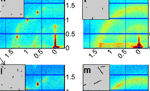
Towards graphene-based spintronics
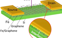 Graphene, a crystalline allotrope of carbon, has remarkable properties including; enormous charge carrier mobility, high thermal conductivity, strong mechanical strength, an electrically tuneable band gap, as well as a long spin coherence length. These last two properties make graphene an ideal semiconductor for the fabrication of the new spin transistor, which will function by the generation and tuning of electron spin polarised currents (spintronics). Spintronics is a technology that uses electron spin, rather than charge, to build faster and more efficient devices. In fact the ability to construct a graphene/ferromagnetic heterojunction is currently one of the most sought after achievements in solid state physics. The nature of this heterojunction has previously been difficult to characterise as the interface is buried beneath many layers of atoms. Read More
Versatile Soft X-Ray beamline, VERSOX
The main development on the horizon for the Surfaces and Interfaces village is the new Versatile Soft X-Ray beamline, VERSOX (B07), which is scheduled to come online in September 2016. The beamline’s end station has already been commissioned at I09 and achieved pressures of up to 7 millibar. It is expected that this will be extended to pressures of up to 30 millibar within the next year, enabling studies to be carried out in liquid water environments. Ultimately the branch will offer users the capability of performing experiments at pressures of up to 100 millibar, and all components have been tested under these conditions. A collaboration with Professor Helen Fielding at University College London (UCL) is currently underway to look at enabling studies of liquid jets at the beamline, which will extend the capability of the beamline further. It is hoped this installation will be complete by the end of 2016, giving users the ability to study liquid-gas as well as solid-gas interfaces.
Figure 1: B07 end station.
The last year has seen significant progress in the construction of B07. Building work on the beamline’s cabins was completed in June 2015, and installation of the optical components began the month after. The first mirror was installed in December 2015 followed by all the other optical components. First light to the beamline was achieved in April 2016 when the end station was transferred from I09, where it had previously been open to users.
The second branch of B07 is currently in design stage. Operating independently of the first branch, it will offer a high throughput X-ray Photoelectron Spectroscopy (XPS) system at an end station equipped with a robotic sample changer, allowing automatic screening of samples. Moderate vacuum restrictions will be in place, facilitating the characterisation of samples related to heritage conservation, geological specimens, or polymeric electronic materials, which are often incompatible with ultra-high vacuum requirements due to outgassing. Components for this branch have been ordered in preparation for construction in summer 2016.
NanoARPES measurements
The second branch of the Angle Resolved Photoemission Spectroscopy beamline, ARPES (I05), which will host all nanoARPES measurements on the beamline, achieved significant progress last year. Construction of the beamline and end station for the branch have now been completed. Key to this was the installation of the in vacuum motion stages that hold the sample and the a Fresnel zone plate, a focusing element used to de-magnify the 50 – 200 eV beam into a spot of less than 1 μm. Two zone plates have been developed in collaboration with the Paul Scherrer Institute in Switzerland. Following first light in November 2015 the beamline has been undergoing fine-tuning and welcomed first users in April 2016.
The new instrument is optimised for nano-ARPES scanning microscopy, with an ultimate resolution of 0.3 μm and allows full ARPES data acquisitions, albeit at reduced energy resolution, to be acquired from a small spot. It employs a combination of a secondary electron detector for fast microscopy with a large hemispherical analyser for high transmission and high-resolution ARPES acquisitions. The analyser’s angle-multiplexing lens can rotate around the sample spot to measure the full-cone angular distribution of photoelectrons, which yields the full Fermi surface mapping information from the probed spot.
 Figure 2: The new nano-ARPES branchline on I05.
HAXPES end station
This year will see the final installation of a dedicated Hard X-ray Photoelectron Spectroscopy (HAXPES) end station at the Surface and Interface Structural Analysis beamline (I09).
HAXPES, which uses hard X-rays to achieve greater penetration depths, gives users the ability to study interfaces deeper within samples. HAXPES measurements are currently carried out on the main I09 end station but by developing a dedicated and optimised end station for the technique the beamline will be able to serve more users in both HAXPES and surface techniques.
The HAXPES end station will be installed in experimental hutch one on the beamline’s hard X-ray I branch. The designs for the end station are almost complete and components, including a KB (Kirkpatrick-Baez) mirror, were delivered for assembly in March 2016. The end station is being designed to ensure it can support a range of sample environments, for example gas cells or magnetic environments. The final installation of the end station is planned for October 2016, with first users expected in 2017.
New end station at I10
BLADE, the Beamline for Advanced Dichroism Experiments (I10) currently hosts two end stations. The first end station has a high field superconducting magnet capable of reaching 14 Tesla. However while the station is capable of generating large fields, suitable for studying magnetic materials, it is unable to produce a true zero field, only being able to reach within 10 mTesla of this.
In order to rectify this situation a third end station with a smaller electromagnet of up to 2 Tesla is under development. As with the high field magnet this third end station will be optimised for absorption measurements. However the smaller field will allow better control close to zero field, opening up true zero field measurements which are advantageous for measurements of technologically applicable samples. In addition a cryostat will allow cooling down to less than 10 K to access low temperature phases. The magnet arrived in March 2016, and the new end station is expected to come online for users by October 2016.
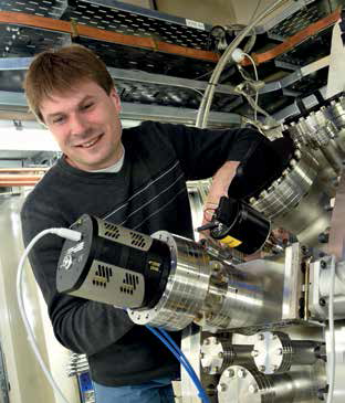
Figure 3: Paul Steadman, Principal Beamline Scientist, on BLADE, I10.
This year has seen the village make significant progress in increasing the range of sample environments for users, a trend that is set to continue in the coming year, especially when the new beamline, the Versatile Soft X-Ray beamline (B07) comes into use. The village is also set to increase the capability of the Hard X-ray Photoelectron Spectroscopy (HAXPES) and nanoscale Angle Resolved Photoemission Spectroscopy (nanoARPES) techniques in the next year.
The Angle Resolved Photoemission Spectroscopy beamline, ARPES, (I05) uses a vacuum ultraviolet (VUV) to soft X-ray beam to study the electronic structure of crystalline solids and their surfaces at less than 100 x 100 μm spot size. Thanks to the cleavage method, which allows the majority of users to quickly prepare sample surfaces directly on the beamline, this has been another very productive year for I05, with an average of two papers a month being published by users using this method. For those unable to use the cleavage method, I05 also supports users that prepare samples in situ. Over the last year, significant progress has been made to commission a second branch and end station for I05, which will support nano-ARPES measurements. The new branch achieved first light at the end station in November 2015 and welcomed first users in April 2016. Together the two branches will support users studying materials such as non-conventional superconductors, topological matter and transition metal chalcogenides.
The Nanoscience beamline (I06) produces polarised soft X-rays in the 80 – 2000 eV range and supports soft X-ray diffraction and spectroscopy. It combines microfocused soft X-rays with variable linear and circular polarisation and X-ray photoelectron emission microscopy (PEEM) to provide spectroscopic data on nanometre length scales. The intense polarised beam can be focused to a spot several micrometers in diameter, allowing the PEEM to probe nanomagnetism and nanostructures. The beamline can also support the study of processes on a picosecond timescale. The beamline images at high spatial resolution using polarised XAS or XPS. A motorised sample stage at the PEEM end station allows users to efficiently move over the surface of a sample in a reproducible way. The beamline is particularly suited to the study of magnetic materials, and studies in the last year include imaging antiferromagnetic domains in the multiferroic material - bismuth ferride.
The Surface and Interface Diffraction beamline (I07) is currently the only beamline in the village that is not limited to studies in vacuum. Using hard X-rays of 8 to 30 keV allows penetration through to deeper interfaces of interest, opening up the possibility of studying electrochemical reactions and liquid-liquid interfaces. The beamline supports X-ray scattering studies including Grazing Incidence Small Angle X-ray Scattering (GISAXS), X-ray Reflectivity (XRR) and Surface X-ray Diffraction (SXRD) techniques. To date, the main bottleneck for the beamline has been its software. As a result significant efforts are being made to improve and simplify analysis for the non-specialist user. In the coming year, a number of new sample environments are being developed including MINERVA, a chamber for in situ small organic molecule deposition that can be used for applications such as photovoltaics. A number of environmental chambers for controlled atmospheric gas or liquid environments are also being developed. Users will have the ability to heat samples in these new chambers, allowing them to mimic environments such as those found in solid oxide fuel cells.
The Surface and Interface Structural Analysis beamline (I09) is unique in being the only beamline in the village to utilise both soft and hard X-rays concurrently. By combining soft X-rays (100 - 1200 eV) with hard X-rays (2.35 keV to ≥15 keV) users can combine a larger number of techniques for sample analysis of the same spot. Techniques supported by the beamline include XPS, Near Edge X-ray Absorption Fine Structure (NEXAFS), X-ray Standing Waves (XSW), Photoelectron Diffraction (PhD) and XRR. The beamline also supports HAXPES. I09 is particularly well suited for the study of layered materials such as metal oxide heterostructures, where users can probe deeper into their sample as well as investigating the surface structure. Over the last year, a new soft-X-ray branch was commissioned for I09, while a second preparation chamber and ultra high vacuum storage chamber were added to the existing end station. The coming year will see a dedicated HAXPES end station added to the beamline, increasing user capacity for measurements on I09.
BLADE, the Beamline for Advanced Dichroism Experiments (I10) is a polarised soft X-ray beamline in the energy range of 400 – 2000 eV. It allows for the study of magnetisation and the magnetic structure of novel nanostructured systems. I10 mainly supports materials and physics research such as the study of thin magnetic films, multiferroics and topological insulators, but also hosts biological applications, such as how metals interact with proteins in the brain in individuals with Alzheimer’s. I10 currently consists of two end stations - an absorption branch with a high field magnet and a scattering branch with a diffractometer. A third end station that will allow users to carry out zero field measurements is underway and scheduled to be working by October 2016.
VERSOX (B07) will be the newest addition to the Surfaces and Interfaces village, offering XPS and XAS at high pressures, currently tested up to 7 millibar, but ultimately reaching 100 millibar. It is due to open for users in September 2016. When ready the beamline will offer users the ability to carry out atmospheric chemistry, catalysis, and biological investigations under native conditions such as liquid environments. The last year has seen significant progress to the beamline’s construction. In 2015, the end station was commissioned at I09 and open to users from February 2016 until March 2016. It is expected that this will enable a fast transfer of the end station when the beamline at B07 is commissioned later in the year.

Diamond Light Source is the UK's national synchrotron science facility, located at the Harwell Science and Innovation Campus in Oxfordshire.
Diamond Light Source Ltd
Diamond House
Harwell Science & Innovation Campus
Didcot
Oxfordshire
OX11 0DE
Copyright © Diamond Light Source. Diamond Light Source® and the Diamond logo are registered trademarks of Diamond Light Source Ltd
Registered in England and Wales at Diamond House, Harwell Science and Innovation Campus, Didcot, Oxfordshire, OX11 0DE, United Kingdom. Company number: 4375679. VAT number: 287 461 957. Economic Operators Registration and Identification (EORI) number: GB287461957003.