High-speed X-ray imaging reveals complex behaviour during metal 3D printing
Aug 1, 2019
Aug 1, 2019
Related publication: Leung C. L. A., Marussi S., Atwood R. C., Towrie M., Withers P. J. & Lee P. D. In situ X-ray imaging of defect and molten pool dynamics in laser additive manufacturing. Nat. Commun. 9, 1355 (2018). DOI: 10.1038/s41467-018-03734-7
Publication keywords: Additive manufacturing; Defect; Molten pool dynamics; High-speed X-ray imaging
A type of 3D printing called laser additive manufacturing (LAM) uses a high-energy laser beam to melt powder particles into a solid structure in under 1/1000th of a second. The powder melting process controls how materials are formed, governing the overall product performance. However, the fast laser-material interaction makes it difficult to optimise the processing conditions, resulting in defects. The presence of defects slows down the adoption of LAM for safety-critical engineering components such as turbine blades, energy storage, and biomedical devices.
Laser additive manufacturing (LAM), or metal 3D printing, transforms a 3D digital design into a real-life component by fusing metallic, ceramic, or other powders using a laser beam, layer-upon-layer. It has been used for a wide range of product applications, including jewellery, sports equipment, dental implants, and fuel nozzles. The adoption of LAM in the production of safety-critical engineering structures, such as turbine blades, biomedical, and energy storage devices, is hampered by many technical challenges1, including complex laser-matter interactions2, powder oxidation3, and defects4, such as porosity and spatter. These defects may act as stress initiators, deteriorating the performance of LAM components during use. A better understanding of how these defects are formed and evolved during LAM is crucial for process and product optimisation.
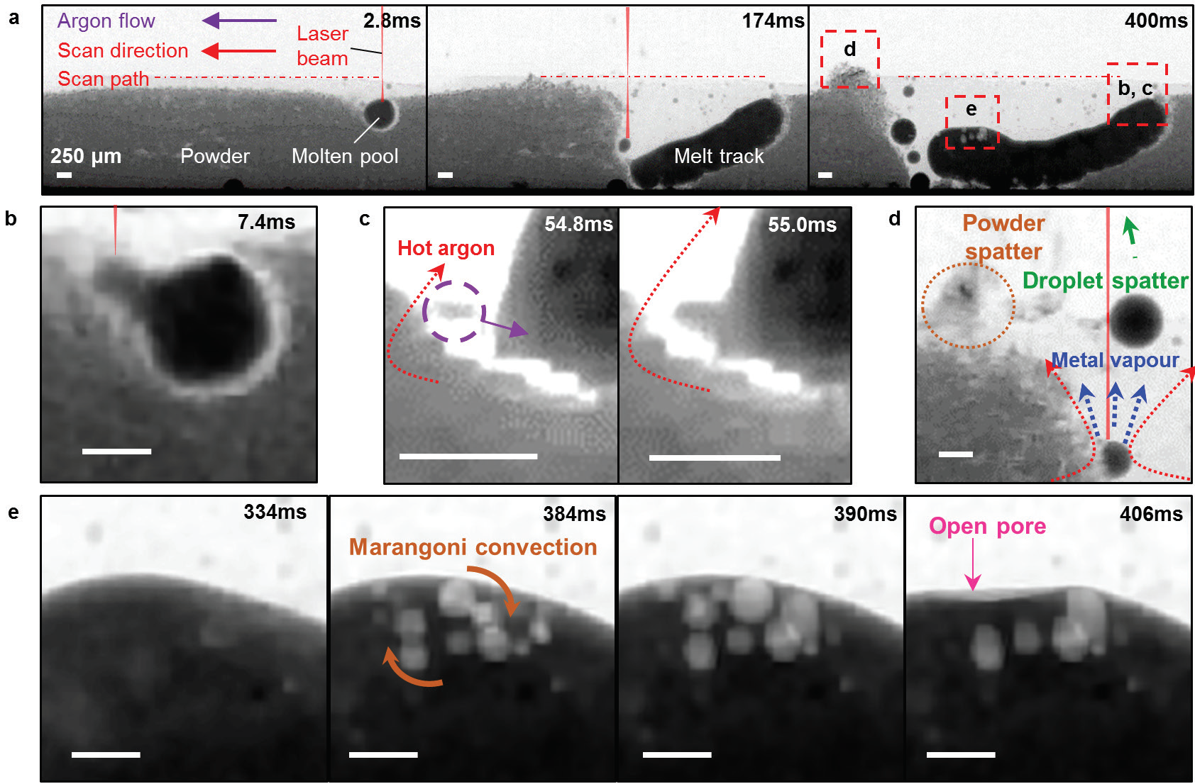
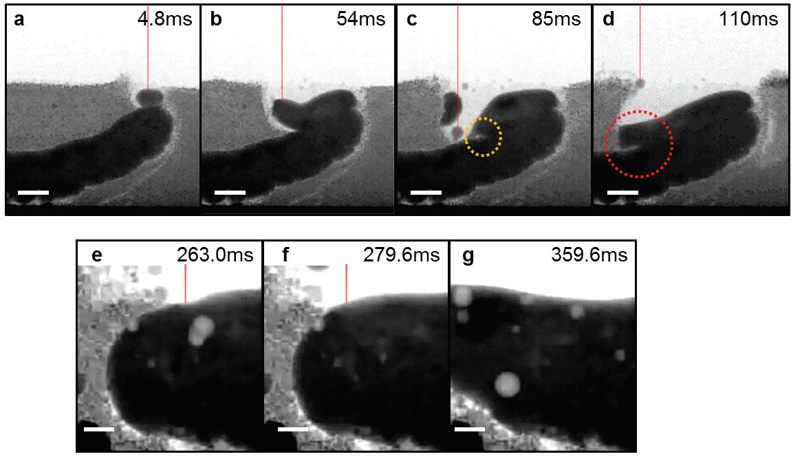
At present, the underlying defect formation mechanisms are inadequately understood, because the laser-matter interaction, and subsequent thermophysical phenomena, occur on very short time scales (10-6 - 10-3 s). Although some phenomena at the powder bed surface have been revealed by in situ process monitoring devices during LAM, the evolution of defects inside a molten pool (or melt tracks) has not been observed, hindering our understanding of LAM.
Third-generation synchrotron radiation sources, such as Diamond Light Source, provide high-energy and high-flux X-ray beams for high-speed imaging with high temporal (~10-3s) and spatial (~10-6m) resolution. They have been used to provide insights into a wide range of dynamic processes, including semi-solid forming, laser processing, battery failure, and volcanic eruptions. In this study, a LAM process replicator2 and synchrotron X-ray imaging were used to investigate defect and molten pool dynamic behaviour during LAM of Invar 36 powder. Invar 36 is a material of interest for precision instruments, optical devices, and aircraft tooling owing to its low coefficient of thermal expansion.
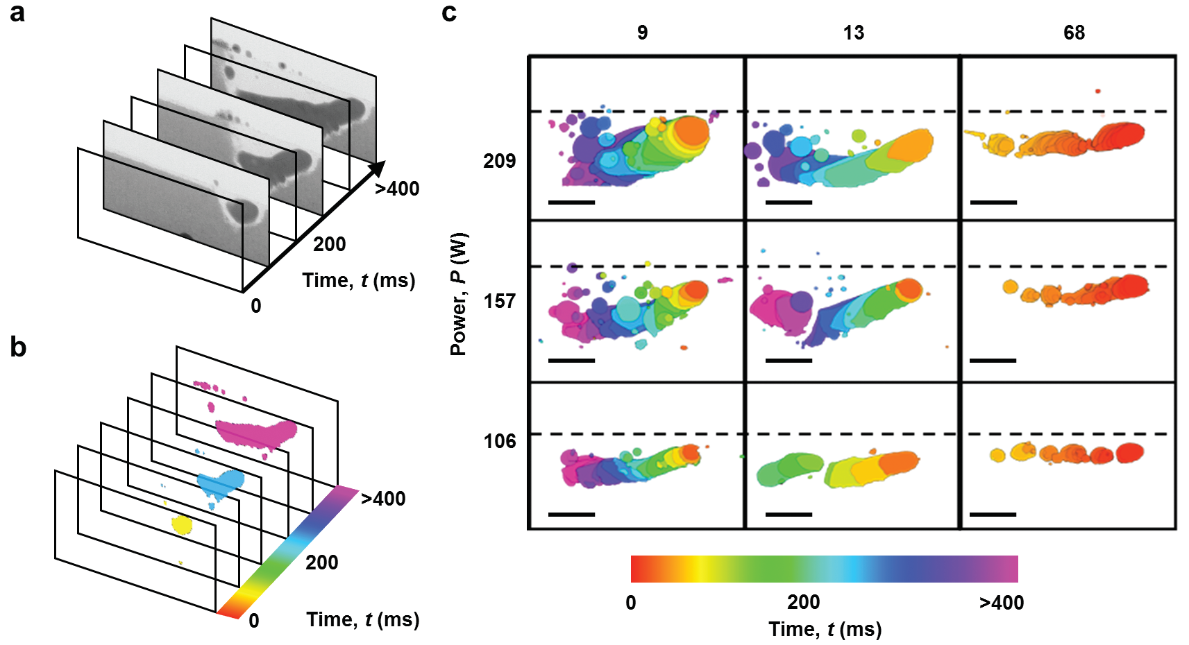
A mechanism map (Fig. 2) is developed to encapsulate the evolution of melt features, and the underlying thermophysical phenomena occur in a systemic set of LAM trials. It highlights an increase in laser power that would transfer more laser energy to the powder particles and the melt track, resulting in a violent movement of liquid metal, a frequent spatter ejection, and a deeper melt track. With increasing scan speed, less laser energy is delivered to the powder bed, lowering the temperature of the melt features while increasing their surface tension. As a consequence, the track morphology changes from a continuous hemi-cylindrical track to disconnected beads. This map emphasises the relationship between processing parameters, molten pool dynamics, and track morphology. It can be applied to other materials, processing conditions, or manufacturing processes, helping end-users to develop a more efficient processing environment.
References:

Diamond Light Source is the UK's national synchrotron science facility, located at the Harwell Science and Innovation Campus in Oxfordshire.
Diamond Light Source Ltd
Diamond House
Harwell Science & Innovation Campus
Didcot
Oxfordshire
OX11 0DE
Copyright © Diamond Light Source. Diamond Light Source® and the Diamond logo are registered trademarks of Diamond Light Source Ltd
Registered in England and Wales at Diamond House, Harwell Science and Innovation Campus, Didcot, Oxfordshire, OX11 0DE, United Kingdom. Company number: 4375679. VAT number: 287 461 957. Economic Operators Registration and Identification (EORI) number: GB287461957003.