Understanding the behaviour of electrons in spintronic materials
Jun 1, 2018
Jun 1, 2018
As the interface between magnetic and non-magnetic materials is a key feature of spintronic devices, it is crucial to characterise and understand both the surface and bulk electronic and magnetic properties of the materials used in their production. For transition metal oxides it appears that thicknesses on the scale of several nanometers are critical for the appearance or disappearance of desired properties, but the presence of these critical thicknesses is extremely difficult to assess.
Complex materials at the focus of modern research display unusual characteristics, often termed as quantum properties. In many cases, these exhibit a critical dependence on small variations of external parameters such as temperature, electric and/or magnetic field, photoirradiation and strain. Spintronics is a highly active field, exploiting quantum properties to achieve simultaneous manipulation of transport and magnetic ordering, with the perspective of realising extremely compact and efficient devices.
It often difficult to understand whether critical thicknesses arise from intrinsic effects, controllable by interface engineering, or from extrinsic, uncontrollable processes. Such a problem indeed requires the resolution of the electronic structure of a single system, and virtually a single sample, by a technique of intrinsic probing depth tuneable across the surface region.
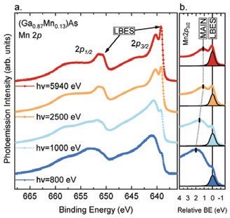
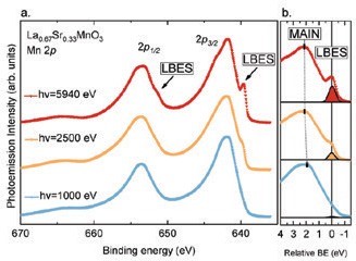
An effective approach has been achieved by the study of core-level satellites in photoelectron spectroscopy (PES)4,5. Indeed, during the photoemission process, photoionised atoms are projected in a set of final states depending on the mechanisms available to screen the core charge, giving rise to satellites. A subset of these, observed at lower binding energy than the main line (low binding energy satellites, LBES), is sensitive to carrier mobility. Cluster-model calculations4,5 define such sensitivity with the hybridisation parameter, which quantifies the contribution of mobile states to the equilibrium electronic structure.
This possibility is offered by the combination of hard and soft X-ray photoelectron spectroscopy (respectively HAXPES and SX-PES) in consistent experimental conditions at Diamond’s Beamline I09. It was applied to two prototypical spintronics systems: the rare-earth-doped manganite, La1-xSrxMnO3 (LSMO), and the most representative diluted magnetic semiconductor, (Ga,Mn)As. In both systems, the relationship between electronic reconstruction and magnetic properties, as well as the competition between electron localisation and hybridisation, are relevant in determining the Curie temperature (TC) and ferromagnetic state.
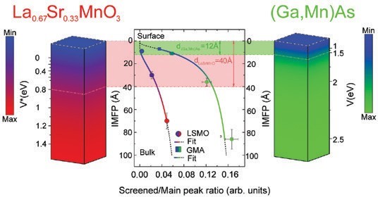
The evolution of the intensity of the LBES versus photon energy could be determined by a line shape analysis (Fig. 1b, Fig. 2b), allowing for the development of a quantification procedure (Fig. 3). The relative amplitude of the LBES component was plotted, for each photon energy, against the corresponding inelastic mean free path (IMFP) of the electrons, defining the corresponding probing depth. The resulting plot was fitted by considering an exponential attenuation of the LBES through the surface layer, whose thickness dwas the fitting parameter. A value d=1.2 nm was found for (Ga,Mn)As and d=4 nm was obtained for LSMO. LSMO was also measured in three strain states induced by substrate mismatch, finding no detectable modifications in d.
The relative energy distance between the LBES and the main line also provided a precise method to compare experiments with state-of-the-art cluster-model calculations, and thus to create (Fig. 3) a vertical scale of the variation of the hybridisation parameter, which, consistently, changed more drastically within the critical thickness in both materials.
In conclusion, it has been demonstrated that the combination of SX-PES and HAXPES can be used to quantify the characteristic scale of the modifications of the electronic structure produced by the surface in complex materials. Such an approach paves the way for methodical discrimination between competing models of the effects of vertical confinement. Finally, precise means to draw a comparison with calculated spectra has allowed reliable attribution of the bulk properties to the increased hybridisation of the ground state with high mobility states.
Funding acknowledgement: This work has been partly performed in the framework of the nanoscience foundry and fine analysis (NFFA-MIUR Italy) facility.
Corresponding authors: Dr Tommaso Pincelli, CNR-IOM, [email protected]. it, Dr Giancarlo Panaccione, CNR-IOM, [email protected]

Diamond Light Source is the UK's national synchrotron science facility, located at the Harwell Science and Innovation Campus in Oxfordshire.
Diamond Light Source Ltd
Diamond House
Harwell Science & Innovation Campus
Didcot
Oxfordshire
OX11 0DE
Copyright © Diamond Light Source. Diamond Light Source® and the Diamond logo are registered trademarks of Diamond Light Source Ltd
Registered in England and Wales at Diamond House, Harwell Science and Innovation Campus, Didcot, Oxfordshire, OX11 0DE, United Kingdom. Company number: 4375679. VAT number: 287 461 957. Economic Operators Registration and Identification (EORI) number: GB287461957003.