 | ||
Competitive growth of fullerene crystals in polymer/fullerene thin-films |
Related publication:
Môn D, Higgins AM, James D, Hampton M, Macdonald JE, Ward MB, Gutfreund P, Lilliu S, Rawle J. Bimodal crystallization at polymer-fullerene interfaces. Physical Chemistry Chemical Physics 17, 2216-2227, doi:10.1039/c4cp04253k (2015).
Keywords:
Polymer nanocomposites; Thin-films; Fullerenes; Organic photovoltaic materials.
The performance of composite fullerene/polymer films, which are potential candidates for the new generation of solar cell technology, is hindered by the growth of large (microscale) crystals. This study of model layered materials shows that crystal growth in a fullerene layer can be carefully controlled by the presence of an adjacent polystyrene (PS) polymer layer. In silicon-supported samples a thinner PS polymer layer promotes the growth of smaller-sized nanocrystals in the fullerene layer, [6,6]-phenyl C61-butyric acid methyl ester (PCBM), which in turn impedes the growth rate of the larger microcrystals. By using a combination of Grazing-Incidence X-ray Diffraction (GIXD) provided by the Surface and Interface Diffraction beamline (I07) and optical microscopy, the relationship between polymer thickness and competitive crystallisation behaviour was examined. To determine the influence of the polymer on this process, complementary measurements used neutron reflectivity to examine the composition of the interface that becomes established between the PCBM layer and the polymer-rich layer, prior to crystallisation. Although the interfacial composition was independent of polymer thickness, a thin polymer layer supported a larger growth-rate for nanoscale PCBM crystals. It is proposed that enhanced nanocrystal growth within the PCBM layer may be due to increased local-polymer-chain-mobility in these nanocomposite thin-films. These results demonstrate the potential significance of free-interface/confinement effects when optimising nano- and micron-scale structure within polymer–fullerene optoelectronic devices such as thin film solar cells. Aside from solar cells, these findings could have important implications for other applications of polymer nanocomposites, include self-healing films and nanocomposite electrolytes.
Surfaces and Interfaces Village | Beamline I07
Crystallisation and mixing are of crucial importance for the performance of polymer/fullerene solar cells1. In this work significant insight into these phenomena is provided, using model amorphous-polymer/fullerene bilayers (polystyrene – PS on top of [6,6]-phenyl C61-butyric acid methyl ester - PCBM). The simplified film morphology of bilayers (cf blends) enables excellent characterisation of local composition and structure, allowing the impact of the polymer layer on crystal growth to be clearly established, and furthering the understanding of the interplay between fullerene crystallisation, polymer/ fullerene mixing and polymer-film-thickness. A number of techniques were used to uncover the behaviour of micron-sized needle-like PCBM crystals2, PCBM nanocrystals3 and PCBM/PS interfaces.
In situ optical-microscopy was used to measure the growth of individual micron-sized, needle-like crystals during annealing (Fig. 1). Fig. 1 shows significant differences in growth-rates as a function of polymer film-thickness, with significantly longer crystals growing for thicker polymer layers. The needle-like crystals show a characteristic shape of growth-curve, in which the growth-rate gradually declines from its maximum value following nucleation. Evidence, from needles that nucleate at different times, suggests that the growth of the needle tips is not being slowed due to any changing property of the growing needle itself, but is instead impeded by changes in the properties (either the composition or the crystalline nano-structure) of the bilayer into which the needle-like crystal is growing.
To investigate the composition-profile normal to the substrate, neutron reflectivity (NR) measurements (not shown) were performed. The needlelike crystals occupy a small area in these experiments, enabling NR to probe the composition-profile of the remaining film into which the needles grow. NR reveals the rapid transfer of PCBM into the polymer layer, and the establishment of a consistent profile between two compositions (pure PCBM and a PS-rich phase containing ~ 10% PCBM), independent of the starting PS-film-thickness. This is suggestive of an equilibrium interface between Surfaces and Interfaces Village Beamline I07 amorphous PCBM and the PS-rich phase.
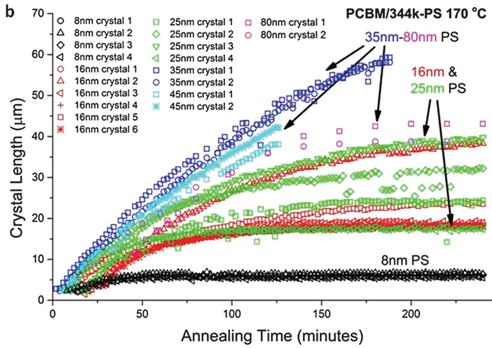
Figure 1: In situ isothermal growth of PCBM crystals for a selection of crystals that nucleate at approximately the same time, for various polymer thicknesses. All samples have a silicon substrate, a 20 nm PCBM bottom layer and a PS top layer. The labels crystal 1 - crystal 6 represent different crystals on the same sample.
The NR results demonstrate that the different growth-rates of micron-sized PCBM needles are not a consequence of differences in PS-thickness leading to large differences in the local composition seen by the PCBM molecules. An alternative explanation for the PS-thickness-dependent growth-rate is that the structure, rather than the composition, within the bilayer is strongly dependent on PS-film-thickness. PCBM nanocrystals are known to form in PCBM thin films and PCBM/polymer blends3. Nanocrystal growth within bilayers was investigated using GIXD (Fig. 2). The unannealed bilayers in Fig. 2 show rings of intensity at |q|~0.7 Å-1 and |q|~1.4 Å-1 corresponding to first and second order diffraction from amorphous PCBM. On annealing there is a clear difference in the diffraction as a function of the PS film-thickness. Diffraction spots are seen after 20 minutes annealing for 8 nm PS, with a further increase in the intensity of these spots after 60 minutes. The GIXD patterns show preferential crystalline orientation with-respect-to the substrate, as observed in PCBM/polymer blends3 and share the strongest intensity peaks with the pure-PCBM film.
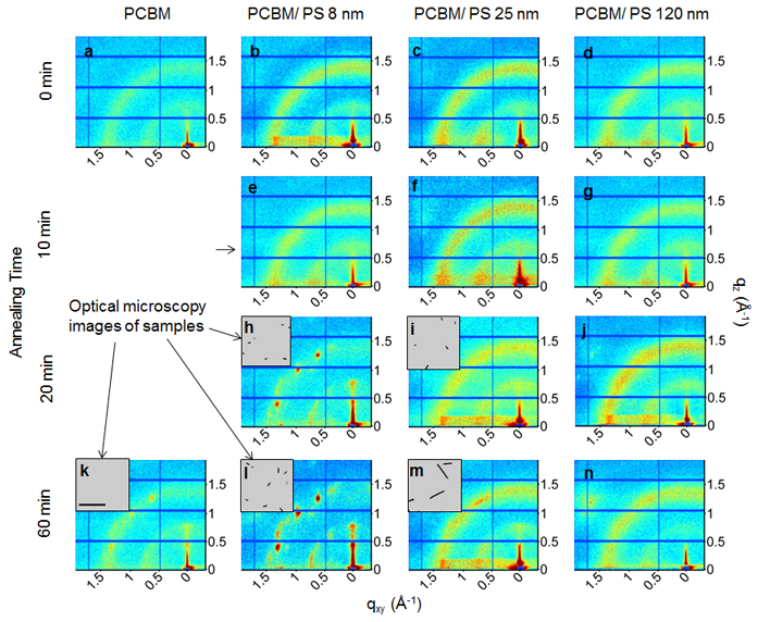
Figure 2: Optical microscopy images and GIXD intensity maps (at an incident angle 0.19˚ – above the critical angle) from PCBM/PS bilayer samples and PCBM single layers on silicon, ex situ annealed at 170 ˚C. a) - n) Direct maps of the detector intensity. The axis labels qz and qxy represent the out-of-plane and in-plane components of the momentum transfer respectively. The scale-bar in the optical microscopy inset in (k) is 20 mm. The optical microscopy insets in (h), (i), (l) and (m) have the same scale as (k).
For 8 nm PS there is a significant reduction in the amorphous PCBM intensity after 20 minutes and a further reduction after 60 minutes. Optical microscopy on these two samples shows needles only cover a small fraction of the sample surface. The 25 nm PS bilayers retain the amorphous PCBM ring, with no evidence of PCBM crystalline spots, after 20 minutes annealing. Optical microscopy shows the presence of needle-like crystals on this sample. By contrast, the annealed pure-PCBM sample shows PCBM diffraction spots, but no observable needle-like crystals. The lack of any correlation between the appearance of diffraction spots and the presence of micron-sized needles demonstrates that the spots are not due to the micron-sized needle-like crystals, but are instead due to crystals within the bilayer that are not resolved by optical microscopy.
The strong influence of the polymer layer thickness on nanocrystal formation, in-parallel with the preservation of an unchanging compositionprofile, suggests that nanocrystal formation is mediated by the polymer at the PS/PCBM interface, but that the nanocrystals, once formed, stay within the ‘bulk’ of the PCBM layer. Such nanocrystal growth within the fullerene layer will impede the growth of the needle-like micron-sized crystals. A simple model, based on the nano-crystalline volume fraction3,4, can be used to quantify the impact of nanocrystal growth on the growth-rate of the needle-like crystals. Fitting this model to the measured growth-curves (Fig. 1) allows nanocrystal growth-rate parameters to be extracted (and compared with approximate values estimated directly from the GIXD measurements) as a function of polymer film thickness. The results show a significant increase in the nanocrystal growth-rate for PS films thinner than ∾30-40 nm.
Comparison with existing reports for mobility enhancement in thin polymer films5 leads to a tentatively-suggested mechanism in which nanocrystalgrowth within the PCBM layer is enhanced, due to increased polymer-chainmobility at the PCBM/PS-rich interface in thin PS/PCBM nanocomposite films.
References:
- Vandewal, K., Himmelberger, S. & Salleo, A. Structural Factors That Affect the Performance of Organic Bulk Heterojunction Solar Cells. Macromolecules 46, 6379-6387, doi:10.1021/ma400924b (2013).
- Yang, X. N. et al. Crystalline organization of a methanofullerene as used for plastic solar-cell applications. Advanced Materials 16, 802-806, doi:10.1002/adma.200306372 (2004).
- Verploegen, E. et al. Effects of Thermal Annealing Upon the Morphology of Polymer-Fullerene Blends. Advanced Functional Materials 20, 3519-3529, doi:10.1002/adfm.201000975 (2010).
- Wong, H. C. & Cabral, J. T. Mechanism and Kinetics of Fullerene Association in Polystyrene Thin Film Mixtures. Macromolecules 44, 4530-4537, doi:10.1021/ma2004458 (2011).
- Keddie, J. L., Jones, R. A. L. & Cory, R. A. Size-dependent depression of the glass transition temperature in polymer thin films. Europhysics Letters 27, 59-64, doi:10.1209/0295-5075/27/1/011 (1994).
Funding acknowledgement:
We thank the staff at the beamlines I07 at Diamond Light Source and D17 at the Institut Laue-Langevin for their support during the experiments. Dyfrig Môn acknowledges EPSRC for funding his studentship via the Doctoral Training Grant to Swansea University.
Corresponding author:
Dr Anthony Higgins, Swansea University, [email protected].
