
Talk Intro: Maria C. Asensio
Aug 16, 2016
Selected presentation abstracts, with an informal introduction from the speakers.
Aug 16, 2016

Synchrotron SOLEIL & Université Paris Saclay
Antares beamline
In today's state-of-the-art material science, length scales play a central role on the chemical and electronic properties of many of the most promising materials for the future. During the last decades, we have witnessed exponential advances in the development of different areas of novel nanotechnologies. These virtuoso materials are often initially isolated or synthetized as small crystallites, which makes difficult their precise exploration. Also, they can be difficult to produce, without fluctuations in their chemical composition, bringing out heterogeneities at variable scales.
Polycrystalline materials, with chemically homogeneous and well-structured grains are also frequent, where the crystalline orientation is challenging to unravel as well as the consequences on the transport and magnetic properties are unknown. In the field of nano-objects also, even if these smart "building blocks" may show remarkable properties, they would have remained unexploited if, we had not developed new tools capable of viewing and scrutinizing ( chemically and electronically) objects on a wide range of scales, from a few microns to a few tens of nanometers.
In the imaging domain, despite the great progress made in spectroscopic microscopy and even the remarkable success achieved, the challenge still remain concerning the precise determination of the chemical and electronic imagery of advances materials, which usually are available as heterogeneous large crystals or tiny homogeneous monocrystals. The challenge is to quantify and analyze the electronic properties of advanced materials on a nano- and micrometer- scale. For such a goal, analysis of the electronic structure must be comprehensive, not only with regard to detection of core levels, but also to disclose the structure of delocalized valence bands, directly responsible for chemical bonds, electrical transport and the thermal and mechanical properties.
Here we report, a recently developed novel X-ray microscope, labelled, k-microscope or Nano-ARPES (Nano Angle Resolved Photoelectron Spectroscopy) recently installed on the ANTARES beamline at the French Synchrotron SOLEIL. This sophisticated instrument is particularly well-suited to provide both high resolved chemical and electronic information in the real and reciprocal space of complex materials with nano-scale resolution. With a spatial resolution of several tens of nanometers, this highly developed microscope is able to carrying out the direct imaging of core levels and their chemical shifts, band electronic structures in reciprocal space and constant energy surfaces in reciprocal space, especially the Fermi surfaces.
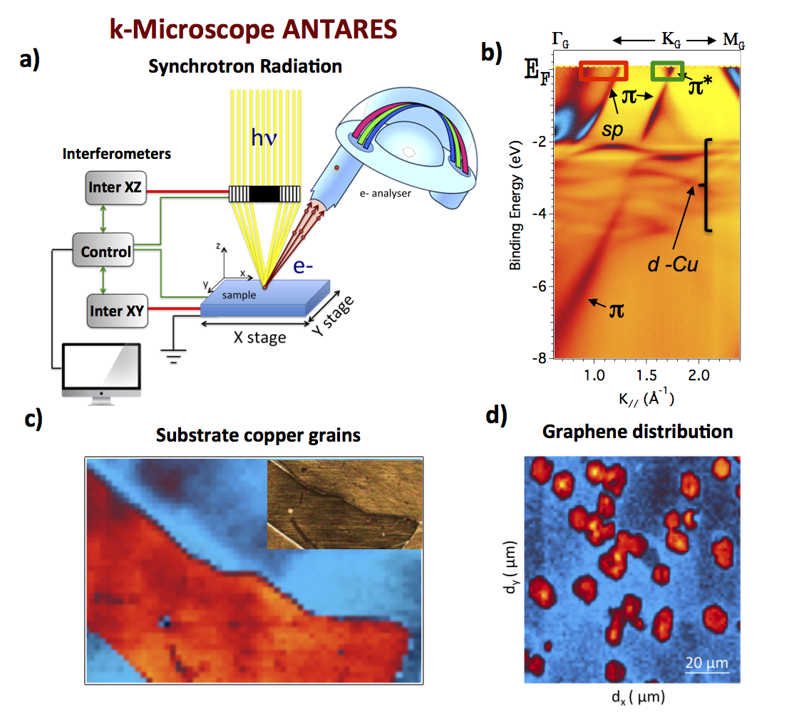
(a) Schematic of the different components of the ANTARES k-microscope. (b) ARPES data showing the “d” and “sp” bands of the copper substrate together with the massless π bands of graphene. (c) real-space image of the copper states intensity (red box states of panel(b)) obtained by nano-ARPES mapping presented on a linear scale as a false-color image. The inset of panel (c) shows the sample optical image where the copper border grains are visible. Panel(d) shows the real-space image of graphene grains distribution, obtained by monitoring the graphene states intensity (green box states of panel (b)).
SURVEYING ELECTRONIC BANDSTRUCTURE OF SMART MATERIALS REVEALED BY NANO-ARPES
Chaoyu Chen, José Avila, Stephane Lorcy,Maria C. Asensio
ANTARES beamline, Synchrotron SOLEIL & Université Paris-Saclay.
L’Orme des Merisiers - Saint Aubin, BP 48 - 91192 - GIF SUR YVETTE Cedex, FRANCE
The use of synchrotron radiation is important for many applications in material science, especially for soft x-ray photoemission spectroscopic experiments. In today’s state-of-the-art angle resolved photoelectron spectroscopy (ARPES) lateral resolution is worse than hundreds of microns. Notwithstanding in advanced materials, length scales from the nano- to the mesoscopic scales dictate and characterize the electronic and other relevant properties. At the Synchrotron SOLEIL, we have recently built a new instrument by combining ARPES principles with scanning microscopy, labeled Nano-ARPES or k-microscope, in which a focused soft x-ray beam is raster-scanned over the samples to create an image one pixel at time while a suitable signal is monitored under computer control, with nano scale resolution, [1]. Figure 1 shows one of our last results on graphene/hBN heterostructrures [2-3].
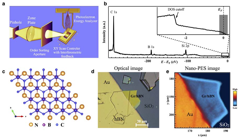
Figure 1: (a) Schematic of focusing for Nano-ARPES. Synchrotron radiation (beam) is focused by Zone Plate (ZP) and selected by Order Sorting Aperture (OSA). The focused spot size on sample is around 120 nm for 100 eV photon energy. The manipulation of sample is realized by a XY scanning controller with interferometric feedback to avoid thermal perturbation. (b), Schematic of G/h-BN lattice structure. (c), Overall photoemission core level spectra taken by Nano-PES with 350 eV photon energy. The inset shows the detailed spectra close to Fermi level. Grey box indicates the energy window used for the Nano- PES image shown in e. (d), Optical image of G/h-BN on SiO2 substrate. The heterostructure is grounded by Au contact. (e), Nano-PES image mapped by scanning the sample along two in-plane axis while collecting the photoelectron intensity by the energy analyzer with energy window set to the Fermi level, as shown in b.
References
 Currently, Permanent Research Staff of the SOLEIL French synchrotron source and Université Paris Saclay, she is also Permanent staff of the Spanish Research Council (CSIC), working in the area of electronic structure of advanced materials. Maria Asensio commenced her academic career in Argentina, where she obtained her PhD in Condense Matter. Then she held several positions at the Autonomous University of Madrid, the University of Warwick and at the Fritz Haber Institute of the Max-Planck in Berlin, Germany. She is author of more than 250 publications, with approximately 4500 cites and more than 100 invited talks in International conferences.

Diamond Light Source is the UK's national synchrotron science facility, located at the Harwell Science and Innovation Campus in Oxfordshire.
Copyright © Diamond Light Source. Diamond Light Source® and the Diamond logo are registered trademarks of Diamond Light Source Ltd
Registered in England and Wales at Diamond House, Harwell Science and Innovation Campus, Didcot, Oxfordshire, OX11 0DE, United Kingdom. Company number: 4375679. VAT number: 287 461 957. Economic Operators Registration and Identification (EORI) number: GB287461957003.