
____________________________________
Industrial Liaison Group:
Tel: +44 (0) 1235 778797
E-mail: [email protected]
Transparent conducting films are an important component of modern life, providing optically transparent and electrically conductive material for a wide range of devices, such as smart phones, touchscreens and solar panels. The field’s most widely used material is tin-doped In2O3 (ITO), accounting for 60% of both global indium use and the transparent conductor market. However, indium is expensive, so there is strong demand for a cheaper alternative or a way to use less indium.
While many previous alternatives to ITO have delivered inferior performance, some transition metal dopants have empirically been found to result in high electron mobilities and conductivities. The challenge is to understand the doping mechanisms of these alternative dopants so that these novel transparent conducting oxides (TCOs) can be optimised.
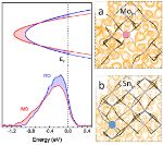
Scientists from the University of Liverpool, UCL and global glass and coatings manufacturer, NSG group, characterised two dopants in In2O3 (molybdenum and tin), comparing the films’ electron mobilities and conductivity as a function of carrier concentration.
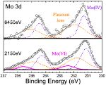
At Diamond’s I09 beamline, hard x-ray photoemission spectroscopy (HAXPES) was used to study the materials. Compared with conventional laboratory-based photoemission with soft x-rays, the high energy photons enhance the relative cross section strength of s-orbitals which dominate the conduction-band emission. This identified different shapes of the conduction-band photoemission spectra in molybdenum based (IMO) and ITO films with the same carrier density. This gave direct evidence of the mixing of tin 5s states with the indium 5s-dominated conduction band minimum (CBM), increasing the effective mass and reducing the electron mobility. Mo 4d states in IMO, in contrast, are seen in HAXPES data in the middle of the band gap and far above the CBM; they have no detrimental effects on the electron transport.
By using HAXPES at Diamond, combined with lab-based techniques and density functional theory, scientists were able to understand the enhanced doping behavior of Mo compared to Sn donors in In2O3. The insight acquired has confirmed that IMO shows higher mobility and therefore higher conductivity than ITO. Therefore, thinner IMO films can be used, reducing indium use. The insights acquired will enable the design of more effective and cheaper TCOs based on doped In2O3 and other metal oxides, leading to better and cheaper products in the electronics and glass coatings markets.
Publication details: DOI: 10.1039/C9MH01014A


“The I09 beamline at Diamond gave us key data on dopant core levels, valence-band states and conduction-band emission which proved vital to developing our understanding of TCO doping by transition metals”.
Prof Tim Veal, University of Liverpool

Diamond Light Source is the UK's national synchrotron science facility, located at the Harwell Science and Innovation Campus in Oxfordshire.
Copyright © 2022 Diamond Light Source
Diamond Light Source Ltd
Diamond House
Harwell Science & Innovation Campus
Didcot
Oxfordshire
OX11 0DE
Diamond Light Source® and the Diamond logo are registered trademarks of Diamond Light Source Ltd
Registered in England and Wales at Diamond House, Harwell Science and Innovation Campus, Didcot, Oxfordshire, OX11 0DE, United Kingdom. Company number: 4375679. VAT number: 287 461 957. Economic Operators Registration and Identification (EORI) number: GB287461957003.

 Industrial Liaison Office