
Images collected at Diamond’s Nanoscience beamline (I06) have helped physicists to investigate the electrical control of magnetism using juxtaposed ferroelectric materials, which is all part of the quest to optimise data storage on the nanoscale.
A major obstacle in the development of electronic devices, particularly microelectronics, is optimising power and performance whilst controlling heat dissipation. Being able to thrash your tablet or laptop for long periods without experiencing overheating could be more than just a pipe dream, as researchers investigate magnetic devices that are controlled by varying an electric field, rather than devices that are switched using magnetic field or electric current. The greatest potential to safely attaining longer battery life is offered by the application of magnetoelectric coupling between materials.

In magnetoelectric systems, electrical and magnetic properties are coupled together. The manipulation of magnetic domains at room temperature is of importance in the developing field of spintronics, in four-state logic devices (NOR gate) and magnetoelectric sensors. Researchers from the University of Cambridge, Diamond, the ISIS pulsed neutron and muon source, and the University of Parma worked together as part of a long-term collaboration with the aim of controlling magnetisation by electrical switching in the absence of an applied magnetic field. Previous work on bismuth ferrite, the only known room-temperature multiferroic, showed that an electric field was able to modify the in-plane (IP) magnetisation of a juxtaposed magnetic film, but switching an out-of-plane (OOP) magnetisation that lies perpendicular to the sample surface presents challenges.
Results from the study have recently been published in Advanced Materials. The team used the Nanoscience beamline at Diamond to perform photoemission electron microscopy (PEEM) on large contiguous areas of nickel films and small exposed regions of barium titanate substrates BaTiO3 (BTO), in addition to using in-house magnetic force microscopy (MFM). PEEM data were obtained with contrast from X-ray magnetic circular dichroism (XMCD) so that the IP and OOP components of magnetisation were imaged simultaneously to provide 3D information. PEEM data were also obtained with contrast from X-ray linear dichroism (XLD) in order to image the ferroelectric domains. Crucially, beamline I06 is able to obtain these two types of image while the voltage is varied across the sample.
Professor Neil Mathur from the University of Cambridge explains the importance of the high resolution imaging and a large field of view offered by I06: "The high resolution was essential for observing the 125 nm-wide magnetic stripe domains in our nickel films, and the large field of view was essential for observing the much larger ferroelectric domains in our barium titanate substrates. The research required two beamtime sessions, and also the know-how that we continue to accumulate through our long-term collaboration with the truly excellent I06 team."
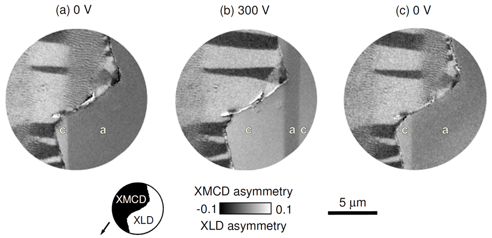
Fig. 1: Photoemission electron microscopy (PEEM) showing high-resolution magnetoelectric images of ferromagnetic and ferroelectric domains that undergo concomitant changes when the latter experiences a change in voltage. The ferromagnetic domains in a film of nickel lie left of the zig-zag edge, and were imaged using contrast from X-ray magnetic circular dichroism (XMCD). The ferroelectric domains in a substrate of barium titanate lie right of the zig-zag edge, and were imaged using contrast from X-ray linear dichroism (XLD).
The research demonstrated systematic electrical and thermal control of OOP magnetisation by creating and destroying OOP anisotropy in large areas of nickel films on BTO substrates. The alternating OOP component of magnetisation in magnetic stripe domains is apparent for any IP sample orientation because the incident x-ray beam impinges upon the nickel film surface at a glancing angle. The change in OOP anisotropy was brought about in a repeatable fashion by overcoming the growth stress with electrically controlled strain from ferroelectric domain switching. Images of ferromagnetic and ferroelectric domains together are rare, and the high resolution was essential for obtaining direct measurements of the nanoscale magnetic stripe domains. Moreover, the magnetic information obtained at Diamond was more complete than it would have been using the traditional scanning microscopy methods of MFM and PFM (piezoforce microscopy).
The results show promise for precise magnetic control over small domains such as in nanopatterned bilayers. Achieving nanopatterned films with individually switchable stripe domains could be employed in low-power data storage. Prof Mathur says “We hope that others around the world will be inspired to exploit the high-resolution magnetoelectric imaging that we have pioneered on I06. We ourselves will explore nanoscale magnets with dimensions similar to our stripe-domain width. These nanostructures could ultimately be exploited for the low-power non-volatile storage of data that is written electrically and read magnetically."
For more information about beamline I06 or to discuss potential applications, please contact Prof Sarnjeet Dhesi: [email protected]
Ghidini, M., Maccherozzi, F., Moya, X., Phillips, L. C., Yan, W., Soussi, J., Métallier, N., Vickers, M. E., Steinke, N.-J., Mansell, R., Barnes. C. H. W., Dhesi, S. S. and Mathur, N. D. Perpendicular local magnetization under voltage control in Ni films on ferroelectric BaTiO3 substrates. Adv Mater. 27 (2015) DOI: 10.1002/adma.201404799

Diamond Light Source is the UK's national synchrotron science facility, located at the Harwell Science and Innovation Campus in Oxfordshire.
Copyright © 2022 Diamond Light Source
Diamond Light Source Ltd
Diamond House
Harwell Science & Innovation Campus
Didcot
Oxfordshire
OX11 0DE
Diamond Light Source® and the Diamond logo are registered trademarks of Diamond Light Source Ltd
Registered in England and Wales at Diamond House, Harwell Science and Innovation Campus, Didcot, Oxfordshire, OX11 0DE, United Kingdom. Company number: 4375679. VAT number: 287 461 957. Economic Operators Registration and Identification (EORI) number: GB287461957003.

 Science