
___________________________________
Industrial Liaison Group:
Tel: +44 (0) 1235 778797
E-mail: [email protected]
Additive manufacturing (AM, also known as 3D printing) allows us to create incredibly complex shapes, which would not be possible using traditional manufacturing techniques. However, objects created using AM have different properties from traditional manufacturing routes, which is sometimes a disadvantage.
Laser additive manufacturing (LAM) uses a laser to fuse together metallic, ceramic or other powders into complex 3D shapes, layer by layer. The cooling rates are extremely rapid, and since they are unlike conventional processes we don’t know the optimal conditions to obtain the best properties, delaying the uptake of LAM in the production of safety-critical engineering structures, such as turbine blades, energy storage and biomedical devices. We need a method to see inside the process of LAM to better understand and optimise the laser-matter interaction and powder consolidation mechanisms.
Based in the Research Complex at Harwell, a team of researchers have worked with scientists at I12, the Joint Engineering Environment Processing (JEEP) beamline and the Central Laser Facility to build a laser additive manufacturing machine which operates on a beamline, allowing you to see into the heart of the process, revealing the underlying physical phenomena during LAM.
Professor Peter Lee from The University of Manchester, who leads the project explains: “The LAM process is very fast, taking place in milliseconds, and to investigate we need microsecond resolution, which can only be achieved with the brilliance of a synchrotron. It allows us to follow the process from powder, through melting and then solidification back into the final solid shape. On JEEP we are investigating the superalloys used in aeroengines, and we need the high energy, hard X-rays produced there to see inside them.”
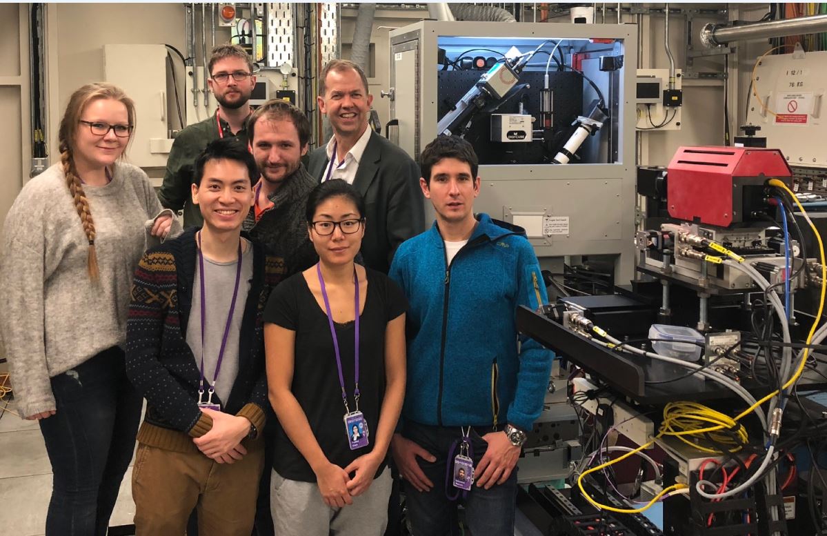
Figure 1: The Additive Manufacturing Team from the Research Complex at Harwell on the Joint Engineering Environment Processing (JEEP, I12) beamline. The Laser Additive Manufacturing Process Replicator (or LAMPR) on the right is used to reveal the underlying physical phenomena during LAM.
In situ, in operando X-ray radiography
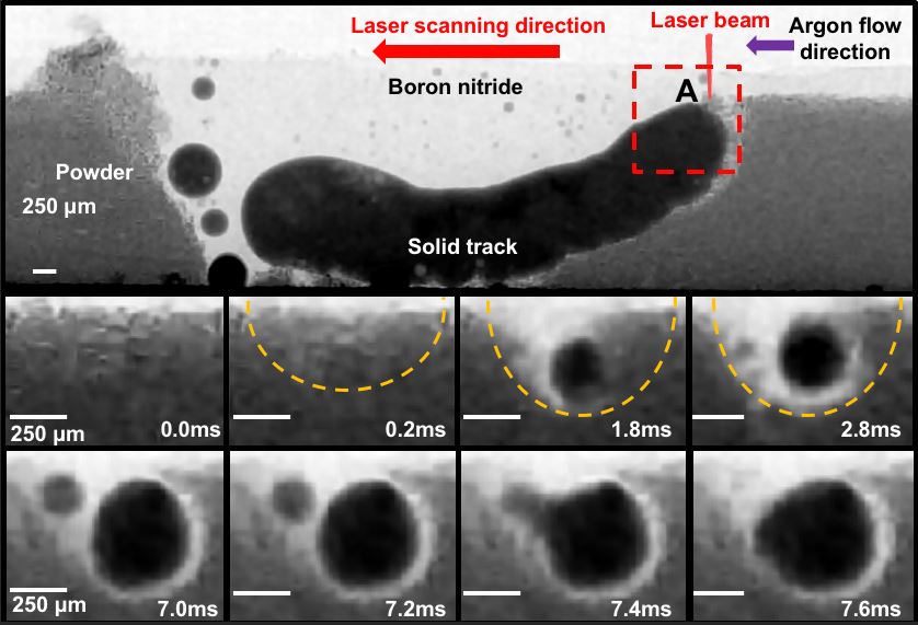
For this research, the team created a novel LAM process replicator, the LAMPR, which allows them to image and quantify the formation of the melt track as the layers are printed during AM. The LAMPR was designed to fit on the beamline and mimics a commercial LAM system, with windows that are transparent to X-rays, allowing scientists to see right into the heart of the LAM process as it takes place. They used X-ray radiography with high temporal and spatial resolution to uncover key mechanisms of laser-matter interaction and powder consolidation during LAM, including the formation and evolution of melt tracks, spatter patterns, the denuded zone (a powder-free zone) and porosity in the deposited layers. The time-resolved quantification of the pore and spatter movements gave crucial information of their flow velocities and direction, which are not possible to acquire using other techniques.
“The LAMPR is a unique piece of equipment, and beamline support was utterly essential. We worked with Diamond staff right from formulating the proposal. Diamond helped with the mechanical design, and the optics and integrating the LAMPR into the control systems”, says Dr Alex Leung, the PDRA leading the experiments.
The results of these experiments clarify aspects of the physics underlying LAM, which are crucial for its development. The previous hypothesis was that the formation of surface porosity on finished objects was due to incomplete melting or insufficient liquid feeding. However, this research shows that it is formed via a pore-bursting mechanism. Pores near the surface escape into the atmosphere, leaving behind a surface depression.
To find out more about X-ray radiography, or to discuss potential industrial applications, please contact the Industrial Liaison team on 01235 778797 or send us an e-mail. You can keep in touch with the latest development by following us on Twitter @DiamondILO or LinkedIn.
Leung ACL et al. In situ X-ray imaging of defect and molten pool dynamics in laser additive manufacturing. Nature Communications (2018). DOI: 10.1038/s41467-018-03734-7.

Diamond Light Source is the UK's national synchrotron science facility, located at the Harwell Science and Innovation Campus in Oxfordshire.
Copyright © 2022 Diamond Light Source
Diamond Light Source Ltd
Diamond House
Harwell Science & Innovation Campus
Didcot
Oxfordshire
OX11 0DE
Diamond Light Source® and the Diamond logo are registered trademarks of Diamond Light Source Ltd
Registered in England and Wales at Diamond House, Harwell Science and Innovation Campus, Didcot, Oxfordshire, OX11 0DE, United Kingdom. Company number: 4375679. VAT number: 287 461 957. Economic Operators Registration and Identification (EORI) number: GB287461957003.

 Industrial Liaison Office