____________________________________
Industrial Liaison Group:
Tel: +44 (0) 1235 778797
E-mail: industry@diamond.ac.uk
Conducting polymers such as poly(aniline) (PANI) have shown great potential for application in flexible electronic devices. They represent an opportunity to utilise low cost, large scale manufacturing processes compared those required to produce inorganic semiconducting materials. However, such polymer based semiconductors suffer structural defects, which significantly limit the conductivity achievable.
Previous investigations have indicated a clear link between the conductive properties and the microstructure of semiconducting materials mediated by supramolecular structure. A major challenge is the control of such self-assembly to optimise material functionality.
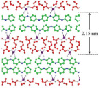
A promising approach to controlling the microstructure is to use oligomers (composed of a few monomers) instead of the polymeric PANI. Researchers at the University of Bristol have used oligo(aniline)s in the presence of an acid surfactant, where the acid surfactant acts both as a dopant and a plasticiser, inducing well-ordered nanoscale phase separation in thin organic films. To understand the supramolecular structure of sub-μm thin films, the team employed surface X-ray diffraction using beamline I07 at Diamond.
The results show that the oligomer-surfactant complexes form highly ordered multilayers parallel to the substrate. The nature of this order depends on: the presence of the surfactant dopant; the molecular architecture of the oligomer and the thickness of the film. The results reveal which parameters are key to the formation of nanoscale structure in semiconducting films and how they may be tailored for use in electronic and optoelectronic devices.
“The unique experimental capabilities and expert technical support at Diamond allow us to perform challenging surface diffraction experiments, investigating a vast array of parameters important to our system, including dynamic processes in real-time. The unprecedented results unravel intricate structural details of our semiconducting oligomer nanofilms, important to their future optoelectronic applications.
Dr Wuge Briscoe and Dr Charl Faul, University of Bristol

Diamond Light Source is the UK's national synchrotron science facility, located at the Harwell Science and Innovation Campus in Oxfordshire.
Copyright © 2022 Diamond Light Source
Diamond Light Source Ltd
Diamond House
Harwell Science & Innovation Campus
Didcot
Oxfordshire
OX11 0DE
Diamond Light Source® and the Diamond logo are registered trademarks of Diamond Light Source Ltd
Registered in England and Wales at Diamond House, Harwell Science and Innovation Campus, Didcot, Oxfordshire, OX11 0DE, United Kingdom. Company number: 4375679. VAT number: 287 461 957. Economic Operators Registration and Identification (EORI) number: GB287461957003.

 Industrial Liaison Office