
Perovskites are crystalline semiconductors that show great promise as solar cell materials. Perovskite-based solar cells have a similar efficiency of converting sunlight into electricity as conventional silicon-based solar cells, but are potentially cheaper and easier to manufacture. Perhaps the simplest method for producing crystalline perovskites involves heating a thin film of a precursor material for about an hour, thereby promoting crystal growth. To produce a perovskite-based solar cell with the highest efficiency, this process needs to produce a smooth film of large, regular crystals, but current processing techniques often produce rough films composed of many small crystallites and possessing small voids.
The Small Angle Scattering and Diffraction beamline (I22) at Diamond Light Source has now been used to investigate in detail how perovskite crystallites form and grow during thermal annealing. This involved using I22 to conduct grazing incidence small-angle X-ray scattering (GI-SAXS), a technique known to be effective at characterising the particles in thin films. The X-ray scattering measurements revealed that the annealing process causes an increase in the number of crystals with sizes of 100–150 nm. Comparisons of the X-ray scattering measurements with electron microscopy images confirmed that improvements in conversion efficiencies were correlated with the formation of structurally-pure perovskite crystals. Further studies with X-ray scattering on new generations of perovskites should produce a general picture of how crystal growth occurs in these materials, helping to determine the processing conditions that produce the best perovskite films with the highest conversion efficiencies.
The development of thin-film solar cell (photovoltaic) devices are of growing interest for the development of low-carbon electricity. In recentyears organometal halide perovskites have become a hot topic in thin-film solar cell research1. Perovskite materials have an ABX3 crystal structure, with the most commonly studied materials being composed of methylammonium lead trihalide (CH3NH3PbX3, where X is a halogen atom such as iodine, bromine or chlorine). It has been shown that perovskites can be used as the light harvesting semiconductor material in solar cells, with a power conversion efficiency (PCE) in excess of 20% 2; a level that outperforms competing classes of next generation photovoltaics.
One of the most widely explored techniques to fabricate a perovskite film is to create a blend of a lead salt and an organic component (e.g., lead (II) chloride and methylammonium iodide) that is dissolved in a common solvent such as dimethylformamide (DMF) and cast to form a thin film, typically having a thickness of a few hundred nanometers. Following solution casting of such a ‘precursor’ solution, thermal annealing at 90°C is used to create the final perovskite material. It has been found that the physical structure and morphology of the perovskite semiconductor can have a profound effect on its resultant efficiency when fabricated into a solar cell. In particular, it is known that incomplete surface coverage of the perovskite film can limit a solar cell’s ability to efficiently absorb sunlight. While many microscopy techniques are available to characterise the morphology of semiconductor thin-films, most of them are only sensitive to a film’s surface, and are also unable to distinguish between different crystallites in a complex polycrystalline film. To gain a more complete picture of the structure of such films, it is necessary to use techniques that are sensitive to sub-surface structure. This can be achieved using grazing incidence small angle X-ray scattering (GI-SAXS). This technique can characterise materials structured over mesoscopic length-scales (1 to 100’s of nm) – even when such structure occurs within the bulk of the film. Furthermore, the X-ray high brightness available at modern synchrotrons permits dynamic processes associated with film growth, crystallisation or selfordering to be followed in real-time3.
To gain an improved understanding of how the processing conditions used to ‘grow’ a perovskite film affect its ability to act as a photovoltaic-device applicable material, GI-SAXS measurements were performed at I22 to characterise the formation of a CH3NH3PbI3-xClx perovskite film4. Here,the perovskite precursor solution was first coated onto a surface, with X-ray scattering measurements performed at various times as the film was thermally annealed. Complementary wide-angle scattering measurements (GI-WAXS) were also performed at the XMaS beamline at the European Synchrotron Radiation Facility (ESRF) in Grenoble.
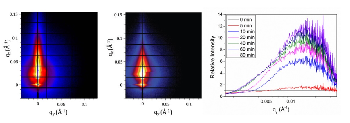
Typical 2D GI-SAXS patterns collected from a perovskite film during thermal annealing at 80°C are shown in Fig. 1a and 1b, with data recorded at times at t = 0 and 120 min respectively. From this, line profiles were determined in the qy direction at the Yoneda Peak. By plotting the data in terms of the change in scattering intensity relative to that recorded at t = 0 min, it is possible observe changes in the scattering profile as a function of time during annealing (Fig. 1c). At t > 40 min, a gradual increase in intensity is observed at length scales greater than ≈ 30 nm. This increase in intensity gradually manifests itself as a peak in the profile centered at ≈ 0.005 °A−1, corresponding to a length scale of ≈ 130 nm. This suggests therefore that as the perovskite is formed from the crystalline precursor phase, there is an increase in the fraction and number of structures within the film having length scales in the range 30 – 400 nm, and in particular an increase in the number of structures having length scales between 100 and 150 nm.
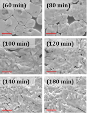
To further investigate the annealing process, scanning electron microscopy (SEM) was used to examine the structure of the films are various times during heating. From the SEM images presented in Fig. 2, it can be seen that as the annealing time is increased from 60 to 120 min, the film evolves from a structure that is dominated by micron-sized grains separated by voids to one composed of many features at smaller length scales (hundreds of nanometers). At annealing times longer than 120 min, the film morphology appears to stabilise and remains comparatively unchanged following further annealing. The significant increase in the fraction of grains having length scales of hundreds of nanometers during the period from t = 60 to 120 min is consistent with the GI-SAXS data shown in Fig. 1.
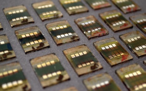
In order to correlate solar cell performance with the evolution of perovskite films during the annealing process, films that were nominally identical to those used for the X-ray scattering measurements were fabricated into complete perovskite solar cells (Fig. 3). It was found that the annealing time increased from 80 to 100 and then 120 min, the average device PCE increased from 7.8% to 10.7% and finally to 12.2%. This increase in efficiency results from an increase in surface coverage, resulting in an enhanced ability of the solar cell to harvest light and also extract charge carriers. GIWAXS measurements performed on the same samples also confirm that the observed increase in PCE is correlated with an increase in the transformed fraction of precursor material to the final perovskite structure.
In summary, the measurements at I22 demonstrate the ability of X-ray scattering techniques to follow the growth of perovskite crystallites in a highly polycrystalline film, with the length-scales determined being consistent with scanning electron microscopy imaging. The results also shed light onto the processes that determine optimum photovoltaic device efficiency. Future experiments are underway to apply similar methods to new generations of perovskite materials that are being developed that have improved efficiency and enhanced operational stability5.
References:
Funding acknowledgement:
We thank the EPSRC for funding this research via the following research grants: ”E-Futures Doctoral Training Centre in Interdisciplinary Energy Research” (EP/G037477/1), ”High resolution mapping of performance and degradation mechanisms in printable photovoltaic devices” (EP/M025020/1) and ”Improved Understanding, Development and Optimisation of Perovskitebased Solar Cells” (EP/M014797/1).
Corresponding author:
Professor David Lidzey, University of Sheffield, d.g.lidzey@sheffield.ac.uk
Related publication:
Barrows AT, Lilliu S, Pearson AJ, Babonneau D, Dunbar ADF, Lidzey DG. Monitoring the Formation of a CH3NH3PbI3-xClx Perovskite during Thermal Annealing Using X-Ray Scattering. Advanced Functional Materials 26, 4934–4942, doi:10.1002/adfm.201601309
(2016).
Publication keywords: Perovskites; GI-SAXS; Photovoltaic devices; Annealing; Crystallisation; GI-WAXS

Diamond Light Source is the UK's national synchrotron science facility, located at the Harwell Science and Innovation Campus in Oxfordshire.
Copyright © 2022 Diamond Light Source
Diamond Light Source Ltd
Diamond House
Harwell Science & Innovation Campus
Didcot
Oxfordshire
OX11 0DE
Diamond Light Source® and the Diamond logo are registered trademarks of Diamond Light Source Ltd
Registered in England and Wales at Diamond House, Harwell Science and Innovation Campus, Didcot, Oxfordshire, OX11 0DE, United Kingdom. Company number: 4375679. VAT number: 287 461 957. Economic Operators Registration and Identification (EORI) number: GB287461957003.

 Science