___________________________________
Industrial Liaison Group:
Tel: +44 (0) 1235 778797
E-mail: [email protected]
Most people will have used a microscope at some point in their life, perhaps in school to observe the wings of an insect or to look at a sample of blood cells. These types of microscopes illuminate the surface of your subject of study and use transparent glass lenses to magnify the image of whatever you are observing. However, the size of the smallest features that can be distinguished under the microscope is on the order of the wavelength of the light used. Visible light, which is the one our eyes are sensitive to, ranges between 390 and 700 nanometres (one nanometre is one billionth of a metre). This means that we cannot observe things that are smaller than a few hundred nanometres using our eyes and visible light.
With the advancement of science and technology, there is a whole world of research that can be carried out on samples at small scales, at just fractions of a nanometre. An electron microscope allows us to see at these small scales.
Electron microscopes are a type of microscope that uses a beam of electrons to create an image of the specimen. It is capable of much higher magnifications and has a greater resolving power than a light microscope, allowing it to see much smaller objects in finer detail. They are large, expensive pieces of equipment, but their immense power has led to great advances in the scientific research world and in particular in the area of biological sciences
By the middle of the 19th century, microscopists had accepted that it was simply not possible to resolve structures of less than half a micrometre with a light microscope because of Abbe’s formula. Ernst Karl Abbe was a German physicist and an optical scientist and he first defined the theoretical resolution of the light microscope and it is his formula (d = λ/2NA) that states that there is a fundamental maximum to the resolution of any optical system due to diffraction.
It was the development of the cathode ray tube that fundamentally changed the way that researchers looked at things; by using electrons instead of light. In 1892, Heinrich Hertz (yes him from the unit of frequency) demonstrated that cathode rays could penetrate very thin metal foil such as aluminium, suggesting that cathode rays were a form of wave motion. Emil Weichert, in 1899, whilst investigating the nature of X-rays, discovered that cathode rays were made up of particle streams. But it was not until 1926 that Hans Busch, another German physicist, showed theoretically that a short solenoid (a type of electromagnet) converges a beam of electrons in the same way that glass can converge rays from the sun, that a direct comparison was made between light and electron beams.
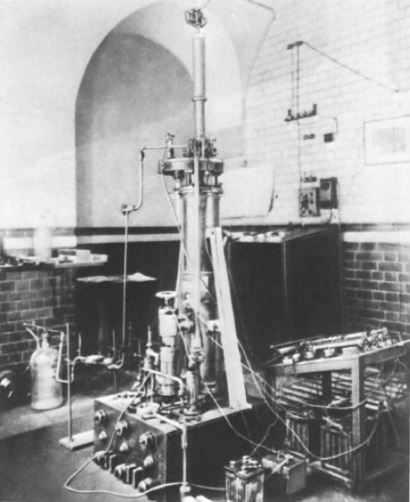
In 1931 the German engineers Ernst Ruska and Maximillion Knoll succeeded in magnifying an electron image. This was in reality the moment of the invention of the electron microscope but the first prototype was actually built by Ruska in 1933 and was capable of resolving to 50 nm. Although it was primitive and not really fit for practical use, Ruska was recognised some 50 years later by the award of a Nobel Prize. The first commercially available electron microscope was built by Metropolitan Vickers and was installed in Imperial College, London in 1936 and was called the EM1. Though it never surpassed the resolution of a good optical microscope, it certainly provided an insight into the challenging problems of design and manufacture of electron microscopes.
Early electron microscopes had a number of issues, the main being that because the electron beam, which had a very high current density, was concentrated into a very small area, it was very hot. It therefore charred any non-metallic specimens that were examined. It wasn't until it was found that you could successfully examine biological specimens in the electron microscope after treating them with osmium and cutting very thin slices of the sample, that the electron microscope began to appear as a viable proposition.
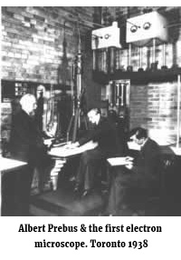 At the University of Toronto, in 1938, Eli Franklin Burton and students Cecil Hall, James Hillier and Albert Prebus constructed the first electron microscope in the New World. This was an effective, high-resolution instrument, the design of which eventually led to what was to become known as the RCA (Radio Corporation of America) range of very successful microscopes. Unfortunately, the outbreak of the Second World War in 1939 held back their further development somewhat, but within 20 years of the end of the war, routine commercial electron microscopes were capable of 1 nm resolution.
The 1940s and 1950s were decades of incremental improvements in instrumentation and technique, with resolution improving as power supplies and lenses were made more stable, and brighter electron guns produced higher-energy electrons to probe the samples. Researchers learned how to prepare specimens of various kinds and to interpret the resulting micrographs. In biology, improved knife-edge microtomes produced thinner and thinner slices of sample that would not be damaged by the electron beam; in materials science, the invention of the replica technique by Mahl in 1941 provided thin enough membranes of plastic or oxide that could be analysed in a TEM (transmission electron microscope).
The years following produced many innovative instruments and trends which opened up a new world of analysis for materials scientists. Ultrahigh voltage TEM instruments in the 1960s and 1970s gave electrons higher energy to penetrate more deeply into thick samples and the evolution and incorporation of other detectors (electron microprobes, electron energy loss spectroscopy (EELS), etc.) made the scanning electron microscope (SEM) into a true analytical electron microscope. Tilting specimen stages permitting examination of the specimen from different angles aided significantly in the determination of crystal structure and computer technology for automated control of electron microscopes and for analysis of the resulting micrographs added to the possibilities of the technology that we use today.
There are two types of electron microscopy; Transmission Electron Microscopy (TEM) and Scanning Electron Microscopy.
Transmission electron microscopy (TEM)
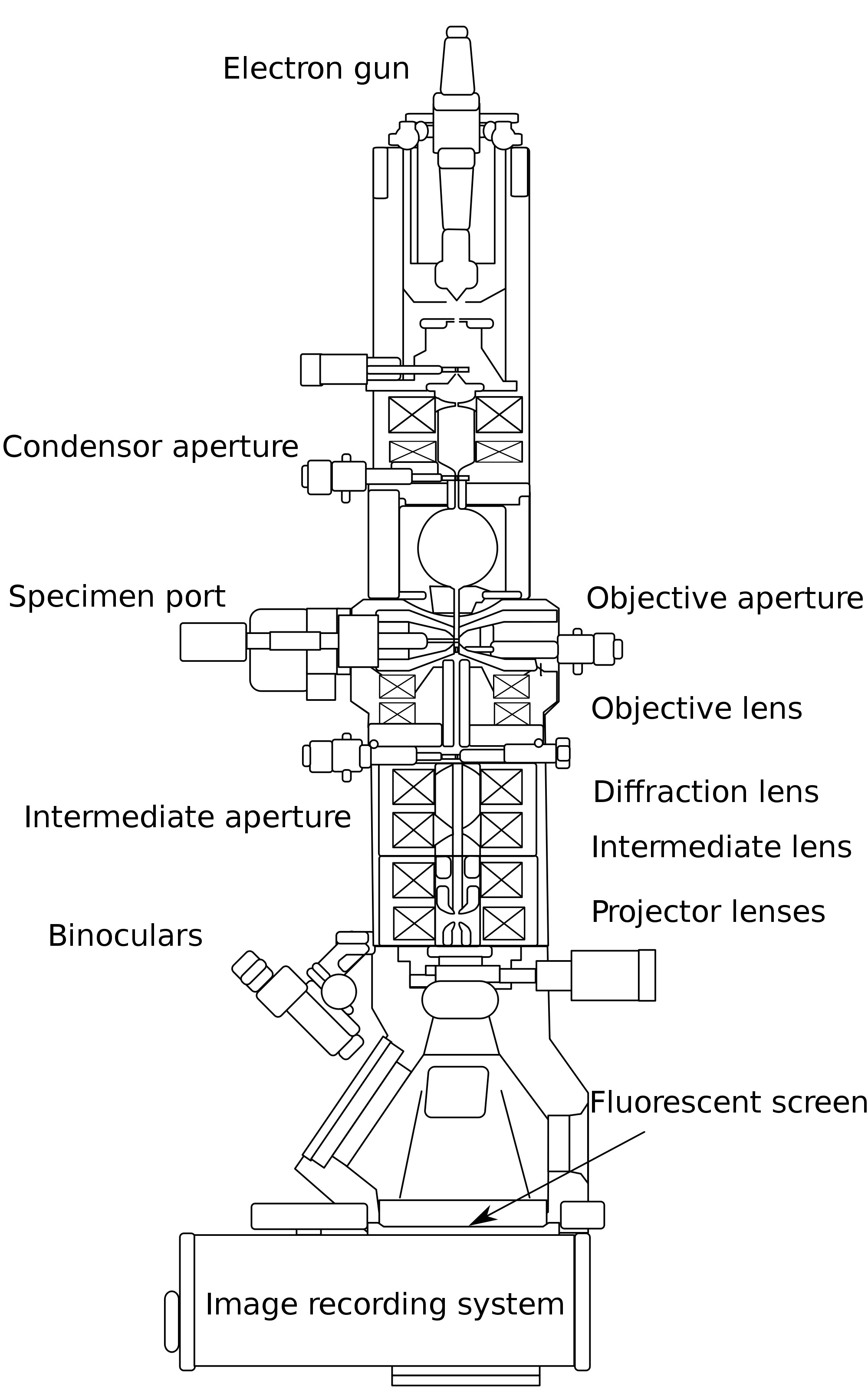 This type of microscopy involves a high voltage electron beam emitted by a cathode and formed by magnetic lenses. The electron beam that has been partially transmitted through the very thin (and so semitransparent for electrons) specimen carries information about the structure of the specimen. The spatial variation in this information (the "image") is then magnified by a series of magnetic lenses until it is recorded by hitting a fluorescent screen, photographic plate, or light sensitive sensor such as a CCD (charge-coupled device) camera. The image detected by the CCD may be displayed in real time on a monitor or computer.
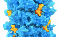
Transmission electron microscopes produce two-dimensional, black and white images. Resolution of the TEM can be limited by spherical and chromatic aberration (an optical effect occurring when the oblique rays entering a lens are focused in a different location than the central rays), but a new generation of aberration correctors has been create that are able to overcome or limit these aberrations. These advances have allowed the production of images with sufficient resolution to show carbon atoms in diamond separated by only 0.089 nm and atoms in silicon at 0.078 nm at magnifications of 50 million times. It is this ability to determine the positions of atoms within materials which has made the TEM an indispensable tool for nano-technologies research and development in many fields, including heterogeneous catalysis and the development of semiconductor devices for electronics and photonics.
TEMs are typically used for viewing internal features that are inside or beyond the surface (e.g. organelles, macromolecules, atoms). It is also possible for TEMs to be capable of 3-D tomography which involves taking a succession of images whilst tilting the specimens through increasing angles, which can then be combined to form a three-dimensional image of the specimen. limitations of TEMs, SEMs yield only greyscale images and it is not possible to observe living specimens as the entire system must be in a vacuum in order for the image to be formed. However, on the plus side, since the SEM image relies on electron interactions at the surface rather than transmission, it is able to image thicker samples and has a much greater depth of view. Hence, SEM images are three-dimensional giving more accurate representations than TEMs.
 Unlike the TEM, at no time does a Scanning Electron Microscope (SEM) carry a complete image of the specimen. Whereas in TEM the electrons in the primary beam are transmitted through the sample, SEM produces images by detecting secondary electrons that are emitted from the surface due to excitation from a primary electron beam. In more detail, SEM works by rapidly scanning your sample with a focused electron beam. This causes electrons to be knocked off the surface of your sample. These secondary electrons provide signals carrying information about the properties of the specimen surface, such as its topography and composition. And it is these secondary or backscattered electrons that are picked up by a detector and are used to produce your image.
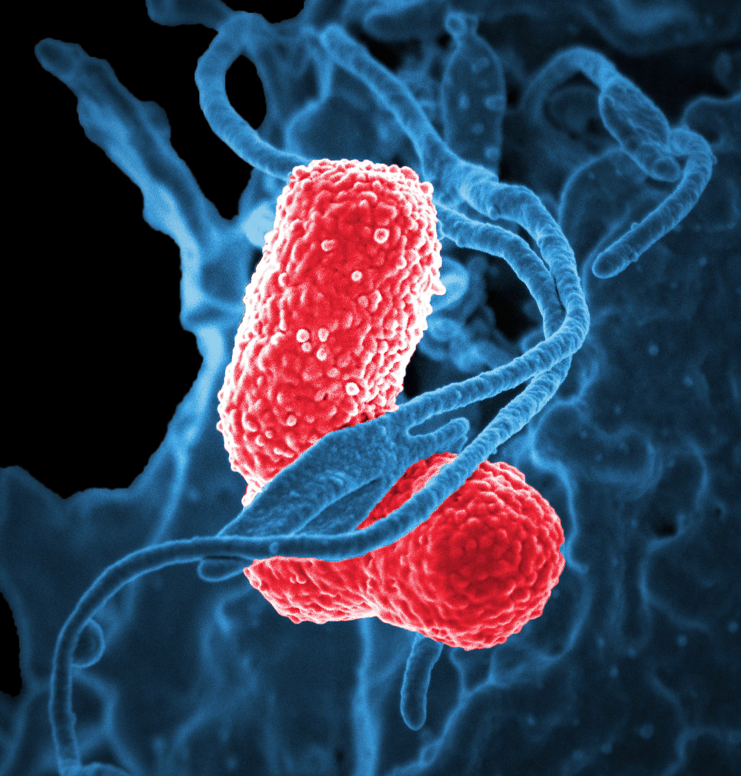
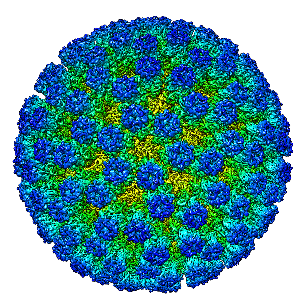
 Cryo-electron microscopy is a method for imaging frozen-hydrated specimens at cryogenic temperatures (-180°C for liquid nitrogen stages, -269°C for He). A tiny drop of the sample is placed onto a copper grid, the sample is 'blotted' to leave a thin layer of molecules and then plunged into something like liquid ethane to freeze it so fast that ice crystals can't form. The grid containing the the frozen molecules is then loaded into the electron microscope and the molecules, when shot with the electron beam, leave a unique "shadow" on the detector. These "shadows" contain all the 3-dimensional information of the molecule, compressed into a 2D image. By combining all the images of molecules in all their various orientations, a 3D structure can be created.
In cryo-electron microscopy, specimens remain in their native state without the need for dyes or fixatives, allowing the study of fine cellular structures, viruses and protein complexes at molecular resolution.
We’re always happy to discuss any enquiries or talk about ways in which access to Diamond’s facilities may be beneficial to your business so please do give us a call on 01235 778797 or send us an e-mail. You can keep in touch with the latest development by following us on Twitter @DiamondILO orLinkedIn.

Diamond Light Source is the UK's national synchrotron science facility, located at the Harwell Science and Innovation Campus in Oxfordshire.
Copyright © 2022 Diamond Light Source
Diamond Light Source Ltd
Diamond House
Harwell Science & Innovation Campus
Didcot
Oxfordshire
OX11 0DE
Diamond Light Source® and the Diamond logo are registered trademarks of Diamond Light Source Ltd
Registered in England and Wales at Diamond House, Harwell Science and Innovation Campus, Didcot, Oxfordshire, OX11 0DE, United Kingdom. Company number: 4375679. VAT number: 287 461 957. Economic Operators Registration and Identification (EORI) number: GB287461957003.

 Industrial Liaison Office