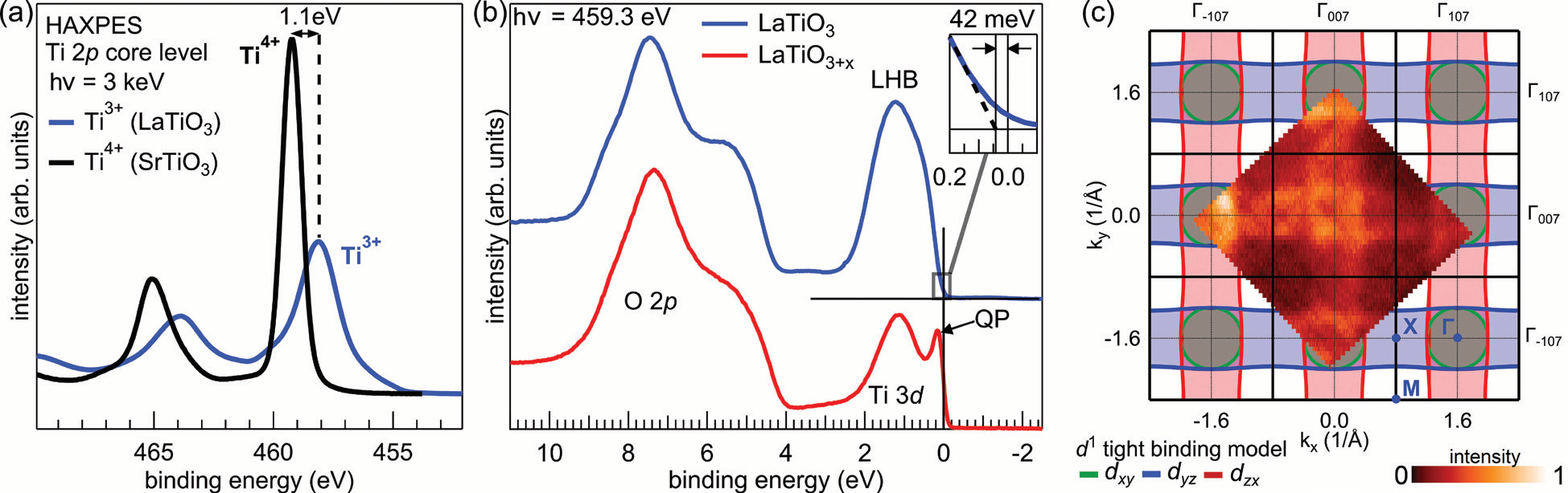
- Figure 2: (a) The titanium valence is monitored by core-level photoelectron spectroscopy of the Ti 2p line. The absence of any sizable Ti<sup>4+</sup> signal in the spectrum from the LaTiO<sub>3</sub> film (blue line) verifies
the correct oxygen stoichiometric; (b) Resonant photoemission at the Ti L absorption threshold allows to investigate the Ti 3d valence band states. Whereas the stoichiometric sample exhibits
a gapped spectrum, the oxygen excess doped thin film is metallic as indicated by the quasiparticle peak (QP) and the Fermi cutoff; (c) Fermi surface measured by resonant SX-ARPES at the Ti L
absorption threshold depicted together with a tight binding model for a filling of d<sup>1</sup>.
Furthermore, I09 provides a UHV suitcase that allows in situ transfer of samples from the growth chamber in Würzburg to the end station at the beamline, which is crucial for the investigations of LaTi3+O3 thin films since the material tends to over-oxidize towards LaTi4+O3.5, corresponding to a reduction of the valence band filling from 3d1 to 3d0. In air the films oxidise in an uncontrolled way impeding any investigations of the dependence of the electronic phase on the oxygen content. Even when the samples are transferred in vacuum, the Ti oxidation state may deviate from its nominal value due to other sources of excess oxygen supplied by, e.g., the substrate, during the growth process, a major challenge that is overcome by a novel growth strategy developed in this study, as discussed in more detail in a related publication4. Therefore, the first experimental task is to verify the stoichiometry of the samples, which can be best characterised by analysing the Ti 2p core level. The comparison of the corresponding spectrum with data obtained from the tetravalent reference material SrTiO3 (Fig. 2a) shows that no sizable amount of Ti4+ ions is present in the LaTiO3 thin films, thereby confirming the intended oxygen stoichiometry and band filling.
The electronic phase, i.e. Mott insulator or correlated metal, is investigated by measuring the Ti 3d valence states using resonant photoelectron spectroscopy (ResPES) at the Ti L absorption threshold. The resonant conditions strongly and selectively enhance the Ti 3d signal, providing a clear view of the valence states. The resulting spectrum of the stoichiometric sample (blue line in Fig. 2b) exhibits a single Ti 3d feature around 1 eV identified as the lower Hubbard band (LHB) and an energy gap at the Fermi level (see the inset in Fig. 2b). Note that, for non-interacting electrons, the configuration of one electron per unit cell would result in a conduction band that crosses the Fermi level. Instead, due to the strong on-site Coulomb interactions between the 3d electrons in a half-filled band, an LHB is formed in LaTiO3 and the material is in the Mott insulating phase.
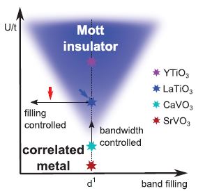
Having demonstrated the Mott insulating phase in stoichiometric samples, the next challenge is to tune the electronic properties in order to reach the suggested operating point for a Mott transistor. As mentioned above, LaTiO3 thin films tend to over-oxidise. This behaviour can be harnessed to reduce the band filling, since every excess oxygen ion accepts two electrons from the Ti 3d states, and thereby drive the Mott transition (see Fig. 1). The effectiveness of this method in p doping and in triggering the Mott transition into a metallic phase is again tested by ResPES. The red spectrum in Fig. 2b shows that, indeed, the LaTiO3+x sample fabricated in higher oxygen pressure exhibits a Fermi cutoff with a quasiparticle peak (QP) characteristic for the correlated metal phase.
The momentum-dependence of the QP spectral weight is further investigated by soft X-ray angular resolved PES (SX-ARPES, Fig. 2c). The corresponding Fermi surface matches approximately the tight binding model of the related correlated metal SrVO3 (Fig. 1). This confirms three important statements about the Mott transition in LaTiO3+x that have been made above. First, the valence electrons form dispersing bands indicative of the metallic phase. Second, the required doping level to reach the metallic phase is rather low, i.e. of the order of only a few percent, since the Luttinger volume of the Fermi surface is still very close to one electron per unit cell (d1). Third, this large Fermi surface shows that indeed all 3d electrons are rendered mobile in the metallic phase and the electronic transport is not related to the doping level as in semiconductor materials.
These findings are not only important steps in material research on the prototypical correlated compound LaTiO3, they also demonstrate that it is a promising channel material for future Mott transistor devices.


 A brighter light for science