

Researchers have discovered a method to improve the functional lifetime and performance of photovoltaic solar cells, which shows great promise for the future of photovoltaics and semiconductors. Using Grazing Incidence Small-angle X-ray Scattering (GISAXS) at Diamond Light Source, the team from the University of Cambridge was able to probe the ordering found in the internal structure of thin films in solar cells, leading to a clearer picture of limiting factors in such systems.
The development of photovoltaics is essential to help reduce the reliance of industrialised nations on fossil fuels. The consensus that sustainable energy production must be increased is a key feature of the ‘Roadmap 2050’ initiative launched by the European Climate Foundation, in preparation for a low-carbon economy in Europe. Semiconductor nanocrystals (NCs) are promising materials for printed optoelectronic solar devices, which could supplement energy production from silicon solar cells. These materials make use of established printing processes and can be produced at low temperatures, reducing the production cost.
Lead chalcogenide nanocrystals already find use in photodetectors, solar cells, displays and transistors. However, their high surface area leaves them susceptible to defect formation, which disrupts charge transport. Additionally, the use of chalcogenide materials in NCs is complicated by disorder introduced when processing the nanocrystal films.
The team has fabricated passivated thin films of nanocrystals containing lead selenide (PbSe), where the film is made more passive to outside influences, in order to protect the voltaic devices from environmental factors that affect device performance. One of the researchers from the University of Cambridge, Dr Alessandro Sepe, tells us: “Despite more than a decade of research, highly performing NC devices are optimised by trial-and-error processing. In particular, detailed knowledge of how the processing of device components determines the assembly of materials, and how this affects electronic properties is lacking.”
“The aim of our research is to gain a fundamental understanding of the formation of mesoscopic morphologies within the photoactive layers, both in terms of their structural and functional properties and their formation kinetics,” Dr Sepe continues. “The principally employed technique is synchrotron GISAXS using the state-of-the-art Surface and Interface Diffraction beamline at Diamond (I07).” The group prepared photovoltaic devices from PbSe-containing NCs that have surface-bound chloride as a result of injection of cadmium chloride after the initial crystal growth period. GISAXS data were used to probe changes in the short or long range ordering of the NCs symmetry in the films’ internal structure. In effect, this explores the chemistry that affects the physics of NC semiconductors, which in turn determines the efficiency of the system.
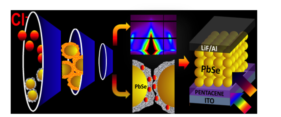
GISAXS (top middle) is a powerful synchrotron technique capable of uniquely resolving the most complex nanostructural properties within the NC systems (bottom middle), proving that chloride treatment (left) confers many benefits on photovoltaic materials (right).
Bilayer solar cells composed of pentacene and PbSe films were analysed following air and solar exposure, to ascertain effects on efficiency and robustness to oxidants or substitution. It was found that the cells containing unpassivated films show a rapid drop in power conversion efficiency, compared to passivated film cells. The distinction is noticeable after just two hours, and after ten hours the passivated cells retain 90% fill factor (efficiency), in contrast to the 50% reduction seen for the unpassivated films.
The GISAXS measurements taken at I07 reveal structural details, offering the potential to control the nanocrystal suprasymmetry and, consequently, the photovoltaic efficiency of NC solar cells. Further advances in overall efficiency are expected through judicious assembly of device materials and through the development of hybrid NC/polymer devices, which are at the interface between inorganic and organic semiconductors. As Dr Sepe says, “Nanocrystals and related organic hybrid materials progressed rapidly from exotic niche materials to vital players in the arena of future photovoltaic materials. Further understanding the structural properties and thermodynamics of NC films and their hybridisation with polymers will be indispensable to the development of highly efficient hybrid solar cells.”
For more information on beamline I07, or to discuss potential applications, contact principle beamline scientist Chris Nicklin: chris.nicklin@diamond.ac.uk
Asil D., Walker B. J., Ehrler B., Vaynzof Y., Sepe A., Bayliss S., Sadhanala A., Chow P. C. Y., Hopkinsons P. E., Steiner U. Greenham N. C. and Friend R. H. Role of PbSe structural stabilisation in photovoltaic cells. Adv Func Mater. (2015) DOI: 10.1002/adfm.201401816
Image credit: 'Solar Panel' by redplanet89 via Flickr under the CC BY 2.0 licence. This is a derivative of the original.

Diamond Light Source is the UK's national synchrotron science facility, located at the Harwell Science and Innovation Campus in Oxfordshire.
Copyright © 2022 Diamond Light Source
Diamond Light Source Ltd
Diamond House
Harwell Science & Innovation Campus
Didcot
Oxfordshire
OX11 0DE
Diamond Light Source® and the Diamond logo are registered trademarks of Diamond Light Source Ltd
Registered in England and Wales at Diamond House, Harwell Science and Innovation Campus, Didcot, Oxfordshire, OX11 0DE, United Kingdom. Company number: 4375679. VAT number: 287 461 957. Economic Operators Registration and Identification (EORI) number: GB287461957003.

 Science