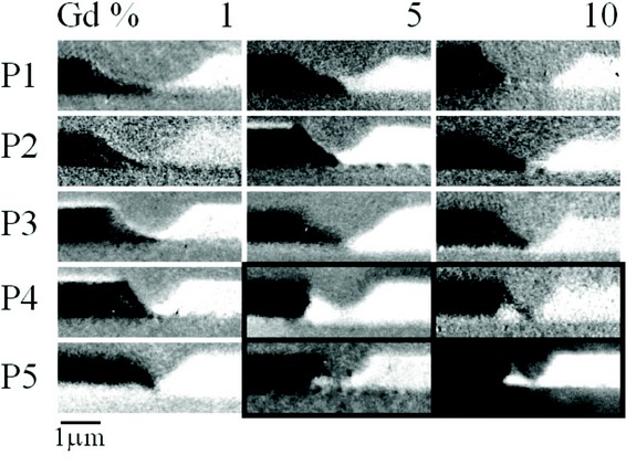
Figure 1: PEEM images showing DW pinning positions for different parabolic pinning potentials and three different Gd concentrations. All constrictions show transverse walls in the centre of the notch except the 5% and 10% Gd samples with notch geometry P4 and P5 (outlined).
Wires with parabolic pinning potentials (see Fig. 1) have been defined using e-beam lithography on Si/SiO2 substrates and obtained by lift-off following sputtering of 20 nm thick Gd-doped Py, with Gd concentrations of 1%, 5% and 10% respectively and a 1.5 nm thick Al capping layer. The parabolic pinning potentials are described by the relation y = cx2 and here we investigate potentials with c/106 values of 0.5, 0.73, 0.91, 1.49 and 3.25 denoted as P1, P2, P3, P4 and P5 respectively. To allow for high frequency measurements the samples were contacted using 10 nm Ta / 140 nm Au waveguide structures defined by optical lithography on top of the wires and connected to a 3 GHz bandwidth vector network analyzer using impedance matched probes.
Domain walls were injected into the pinning potentials using applied magnetic fields and the structure and pinning positions of the domain walls were identified by means of X-ray magnetic circular dichroism combined with photo-emission electron microscopy (PEEM) imaging, carried out at the I06 beamline at the Diamond Light Source synchrotron, using circularly-polarized X-ray photons with energies corresponding to the Fe L3 and L2 absorption edges. The results are shown in Figure 1 for the different pinning potentials and Gd concentrations. We find that the stable domain wall pinning position depends on both the pinning potential steepness and on the Gd concentration. In particular, for Py99Gd1 a transverse domain wall is pinned at the centre of the potential in all cases, as for pure Py. On the other hand for both Py95Gd5 and Py90Gd10 a vortex domain wall is pinned at the side of the pinning potential for the steeper potentials P4 and P5. The preference towards vortex domain wall pinning for higher Gd concentrations indicates an increase in the out of plane magnetic anisotropy, K^, reducing the energy cost of supporting a vortex core. Mixing Gd into transition metals is well known to produce such an anisotropy, and such alloys have long served as magneto-optical recording media. We have confirmed this by measuring the out of plane anisotropy field using vibrating sample magnetometer measurements of 20 nm unpatterned thin film samples of Gd doped Py sputtered on Si/SiO2 substrates.
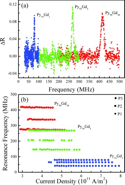
Figure 2: (a) Frequency scans for the P3 potential with a pinned DW at 10 dBm r.f. power and (b) resonance frequencies as a function of current density amplitude for the three different parabolic pinning potentials and three different Gd concentrations.
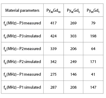
The resonance of domain wall movement driven by an alternating current in the pinning potentials was measured using a vector network analyser where both the amplitude and frequency of the driving current were varied. In this work we concentrate on the pinning potentials which contain a domain wall at the centre of the pinning potential, thus we study the pinning potentials P1, P2 and P3 for Gd concentrations from 1 % up to 10 %. Typical frequency scans for the state with a pinned domain wall are shown in Figure 2a. Each frequency scan was measured at a fixed power by varying the frequency of the applied sinusoidal current, sustained for 1 s at the sample, and measuring the resulting voltage reflection coefficient. Using a transmission line of characteristic impedance of 50 O the sample resistance is then obtained as a function of driving current frequency. The enhanced resistance at resonance, observed as peaks in the scans shown in Figure 2a, arises due to the amplified domain wall movement in the parabolic pinning potentials, resulting in an increase in energy dissipation. The resonance frequency is taken as the centre frequency of the resistance peaks in the frequency scans, and this is plotted as a function of driving current density at the sample for the parabolic pinning potentials P1, P2 and P3 and Gd concentrations 1 %, 5 % and 10 % as shown in Figure 2b with values summarised in Table I. Analysing the results plotted in Figure 2b we distinguish three different effects : i) in all cases the resonance frequency increases as the pinning potential becomes steeper, ii) the resonance frequency is greatly enhanced by increasing the Gd doping percentage for all pinning potentials and iii) the resonance peaks are excited at lower current densities by increasing the Gd doping percentage.
In summary, parabolic pinning potentials provide for harmonic current-induced domain wall resonance and by modifying the magnetic properties of the device material using Gd doping we have demonstrated a method of increasing the resonance frequencies by over an order of magnitude for 10 % Gd doping compared to undoped Py.
Table I : Resonance frequencies, both measured and simulated, for the three different Gd concentrations
Lepadatu, S., Claydon, J.S., Ciudad, D., Kinane, C.J., Langridge, S., Dhesi, S.S. & Marrows, C.H. Tuning of current-induced domain wall resonance frequency using Gd doping, Appl. Phys. Lett. 97, 072507 (2010)
References
- Saitoh, E. et al. Current-induced resonance and mass determination of a single magnetic domain wall. Nature. 432, 203-206 (2004).
- Thomas L. et al. Oscillatory dependence of current-driven magnetic domain wall motion on current pulse length. Nature 443. 197-200 (2006).
- Lepadatu, S. et al. Domain-wall spin-torque oscillators for frequency-selective operation. Physical Review B. 81, 060402 (2010).
Funding Acknowledgement
This research was supported by the ESF EUROCORES collaborative research project SpinCurrent under the Fundamentals of Nanoelectronics programme, and by the EPSRC. We are grateful to the Diamond Light Source for the provision of beamtime.


 Science