

 Diamond Annual Review 2016
 | ||
Towards graphene-based spintronics |
Related publication:
Liu WQ, Wang WY, Wang JJ, Wang FQ, Lu C, Jin F, Zhang A, Zhang QM, van der Laan G, Xu YB, Li QX, Zhang R. Atomic- Scale Interfacial Magnetism in Fe/Graphene Heterojunction. Scientific Reports 5, doi:10.1038/srep11911 (2015).
Keywords:
Spintronics; Graphene; XMCD; Interface.
Graphene, a crystalline allotrope of carbon, has remarkable properties including; enormous charge carrier mobility, high thermal conductivity, strong mechanical strength, an electrically tuneable band gap, as well as a long spin coherence length. These last two properties make graphene an ideal semiconductor for the fabrication of the new spin transistor, which will function by the generation and tuning of electron spin polarised currents (spintronics). Spintronics is a technology that uses electron spin, rather than charge, to build faster and more efficient devices. In fact the ability to construct a graphene/ferromagnetic heterojunction is currently one of the most sought after achievements in solid state physics. The nature of this heterojunction has previously been difficult to characterise as the interface is buried beneath many layers of atoms. For successful spin transport characteristics, and thus a spintronic graphene transistor, there should be no magnetic dead layer at the graphene/magnet interface. Also the magnetic ordering near the interface needs to be stable and not changed by interdiffusion, termination or hybridisation. The problem of how to examine the interface was recently advanced by the use of I10, the Beamline for Advanced Dichroism Experiments (BLADE), at Diamond Light Source where a multi-layer nickel iron ferromagnetic graphene structure (FM1/FM2/graphene) was examined using X-ray Magnetic Circular Dichroism (XMCD) and density functional theory (DFT) calculations. The XMCD data showed an unambiguous ferromagnetic epitaxial Fe/graphene interface that was aided by the inclusion of a Ni stabilising layer on top of the Fe film. This study provides a realistic scenario for graphene-based transistors and the magnetic and electronic nature of the Fe/graphene interface.
Surfaces and Interfaces Village | Beamline I10
As a prototypical two-dimensional quantum system, graphene displays a combination of exceptional properties including; large charge carrier mobility, high thermal conductivity, strong mechanical strength, excellent optical characteristics, electrically tuneable band gap, as well as the recently discovered long spin coherence length. The revolutionary nature of graphene makes it a prime candidate to become a key material for the proposed spin transistors, in which the generation and tuning of spin-polarised currents are prerequisites1. In its pristine state, graphene exhibits no signs of conventional spin-polarisation and so far no experimental signature shows a ferromagnetic phase of graphene. This gap is now being filled up by combined efforts in multi-disciplinary research.
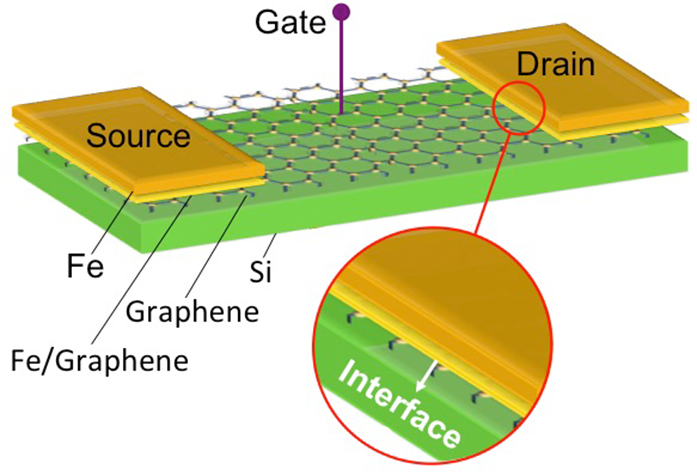
Figure 1: Illustration of the Fe-graphene-based spin field effect transistor and its interface.
The ferromagnetic metal (FM)/graphene heterojunction is one of the most promising avenues to realise efficient spin injection into graphene. In any proposed graphene-based transistors, the best opportunity for spin transport could only be achieved when no magnetic dead layer exists at the FM/graphene interface. Previous studies on various FM/semiconductor (FM/SC) heterojunctions revealed the possibility that the magnetic ordering near a region of the surface or interface of FM/SC may be modified due to interdiffusion, termination and hybridisation; and controversial reports make this issue rather complex2.
Fundamentally all the intriguing spintronic phenomena observed in the FM/graphene heterojunctions strongly depend upon the interfacial hybridisation and magnetic exchange interaction. A direct demonstration of the magnetic and electronic state of the FM/graphene interface down to monolayer (ML) scale remains a nontrivial task, even today, due to the inaccessibility of the buried layer between the topmost atoms and substrate. Moreover, while the FM atoms reduce to a minute amount, many global detection techniques become invalid, as the experimental conditions like vacuum, sensitivity, cryogen etc. must be simultaneously satisfied at a high level. To overcome these obstacles, we employed a unique FM1/FM2/SC structure (in this work, FM1 = 30 ML Ni, FM2 = 1 ML Fe, and SC = graphene)3. The thick FM1 layer provides the FM2 ML with a source of exchange interaction and these two together restore the interfacial behavior of the thick ferromagnetic FM2/ SC. Combined with the unique elemental selectivity of XMCD, such a structure allows direct observation of the magnetisation of FM2 at the FM2/SC interface.
The XMCD of the Fe and Ni L2,3 absorption edges were performed on beamline I10. Circularly polarised X-rays with 100% degree of polarisation were used in normal incidence with respect to the sample plane and parallel with the applied magnetic field (Fig. 1), in order to minimise the nonmagnetic asymmetries and saturation effects. The XAS spectra of the interface Fe and the stabilising layer Ni for both left- and right-circularly polarised X-rays show a white line at each spin-orbit split core level without prominent splitting of the energy, suggesting that the sample has been well protected from oxidation. The spin (mspin) and orbital magnetic moment (morb) were calculated by applying the sum rules to the integrated XMCD and summed XAS spectra of the Fe L2,3 edges4. The mtotal of Fe displays a decreasing trend with the increasing temperature from 1.23 μB/atom at 5 K to 1.12 μB/atom at 300 K, i.e. ∾9% reduction, pointing to a TC close to bulk-like Fe. At the lowest temperature (5 K), we obtained mspin = (1.06 ± 0.1) μB/atom, which is ∾50% reduced from the bulk-like Fe (whose mspin = 2.2 μB/atom) and morb = (0.18 ± 0.02) μB/atom, corresponding to an enhancement of ∾200% compared to morb = 0.085 μB/ atom of that in the bulk. The calculated mspin, morb, and mtotal of the Ni stabilising layer are in good agreement with the previous reports of metallic Ni. The sumrules derived mtotal of Ni exhibits a trend of slight decrease with the increasing temperature from (0.63 ± 0.06) μB/atom at 5 K to (0.52 ± 0.06) μB/atom at 300 K, pointing to a TC close to the bulk-like Ni. Unlike the interfacial Fe, whose morb shows a significant enhancement compared to that of bulk-like Fe, the Ni stabilising layer shows a nearly quenched morb. This is expected for bulk-like Ni, where the effect of the crystal field plays a dominant role5.
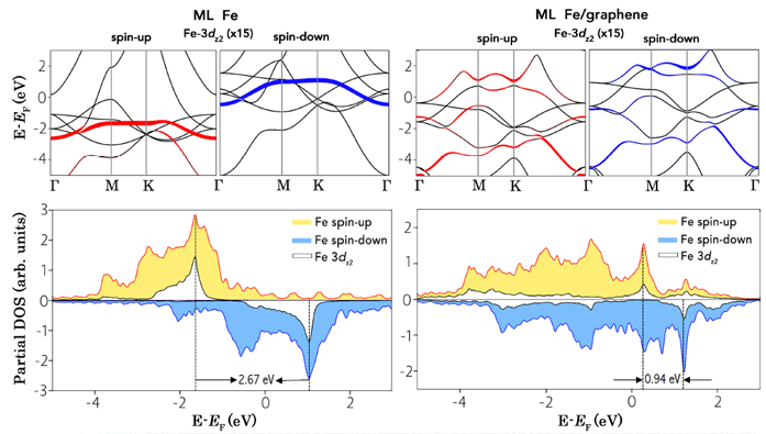
Figure 2: Spin-resolved band structures for a freestanding Fe ML (left column) and the ML Fetop/graphene (right column), respectively, together with their corresponding partial density of states.
The first-principle calculations (Fig. 2) were performed using the projector augmented wave methods implemented in the Vienna ab initio simulation package. In order to determine the electronic and magnetic ground state of the Fe ML on graphene, first it must be addressed where Fe likes to reside with respect to the C atoms. It was found that the Fe atoms deposited on graphene prefer to follow fcc(111) stacking and there exist three inequivalent positions of the fcc Fe allocations on graphene among which the top configuration is most energetically favourable. Consistent with the experiment, the theoretical simulation also reveals a ∾50% reduction in the magnetic moment of Fe. Although Fetop was found the most stable geometry on graphene according to the calculation, the observed numeric results from XMCD, i.e., mspin = (1.06 ± 0.1) μB/atom, is more likely a mixture of Fetop (mspin = 1.23 μB/atom) and Febridge (mspin = 0.67 μB/atom), given the small energy difference (ΔE = 43 meV) of their calculated total energies.
To summarise, we have demonstrated an unambiguous ferromagnetic epitaxial Fe/graphene interface by XMCD. This was aided by the inclusion of a Ni stabilising layer atop the Fe film, which facilitated the study of the temperature dependence of the Fe/graphene interface. Our study restores a realistic scenario of the proposed graphene-based transistors and addresses the open question of the magnetic and electronic nature of the Fe/graphene interface. This approach represents a valuable model of exploring the interfacial magnetism of FM on graphene and the results are encouraging based on the contemporary sample preparation technique. Future work to explore the tuning of the spin polarised band structure of both the FM and graphene via the interface engineering will be of great interest and have strong implications for both fundamental physics and the emerging spintronics technology.
References:
- Geim, A. K. & Novoselov, K. S. The rise of graphene. Nature Materials 6, 183-191, doi:10.1038/nmat1849 (2007).
- Eelbo, T. et al. Adatoms and Clusters of 3d Transition Metals on Graphene: Electronic and Magnetic Configurations. Physical Review Letters 110, doi:10.1103/PhysRevLett.110.136804 (2013).
- Liu, W. et al. Probing the Buried Magnetic Interfaces. ACS Applied Materials and Interfaces 8, 5752-5757, doi:10.1021/acsami.5b11438 (2016).
- Thole, B. T., Carra, P., Sette, F. & Vanderlaan, G. X-ray circular dichroism as a probe of orbital magnetization. Physical Review Letters 68, 1943-1946, doi:10.1103/PhysRevLett.68.1943 (1992).
- Chen, C. T. et al. Experimental confirmation of the X-ray magnetic circulardichroism sum-rules for iron and cobalt. Physical Review Letters 75, 152- 155, doi:10.1103/PhysRevLett.75.152 (1995).
Funding acknowledgements:
This work is supported by the State Key Program for Basic Research of China (Grants No. 2014CB921101 and 2011CB921404), NSFC (Grants No. 61274102 and 21473168), and UK STFC.
Corresponding authors:
Dr Wenqing Liu, University of York, [email protected]; Professor Yongbing Xu, University of York.
